
Your machine vision system captures everything. It does not forgive a missed frame, a corrupt buffer, or a storage bottleneck that shows up six months into a 24/7 deployment. I know this because the gap between a vision system that works in a lab and one that holds up on a factory floor consistently comes down to machine vision storage architecture – not sensor resolution, not lighting, not the inference model. Storage.
Get the frame buffer sizing wrong and you lose data during burst capture. Underspec the write throughput and your pipeline stalls under multi-camera load. Ignore NAND endurance ratings and you are replacing drives six months into a deployment that was supposed to run three years without intervention.
This guide covers the full decision chain, from frame buffer design and sustained write throughput by camera configuration to NAND endurance under continuous imaging workloads, interface selection, environmental ratings, and a product integration path using FORESEE industrial SSDs. At the end, there is a selection checklist you can carry into your next component evaluation.
| Metric | Value | What It Means for Your Design |
|---|---|---|
| DWPD Overconsumption Risk | 3-4x | Direct-write architectures without buffer design regularly exceed rated DWPD by 3x-4x, consuming drive endurance years ahead of schedule |
| Peak Raw Data Rate | 2.16GB/s | A single 12MP camera at 120fps generates 2.16GB/s – no industrial SSD sustains this write rate without a staged DRAM buffer |
| Required Operating Temperature | -40°C to +85°C | Industrial-grade SSDs must cover this full range – commercial drives rated to +70°C fail under real factory enclosure temperatures |
Frame Buffer Architecture in Machine Vision Storage Design
Frame buffering sits at the intersection of sensor output, processing pipeline latency, and storage I/O capacity. The buffer is the bridge between what the camera captures and what the system can write to persistent storage. Design it wrong and the entire data path collapses under load.
There are two primary buffer strategies in machine vision deployments – on-sensor buffering and off-sensor buffering – and the tradeoffs between them affect every downstream storage decision you make.
On-Sensor vs. Off-Sensor Buffering
On-sensor buffering uses DRAM embedded within the image sensor itself to absorb burst capture sequences before transferring data to the system. High-speed sensors like Sony’s Stacked CMOS IMX series include on-chip DRAM for exactly this reason: They can capture hundreds of frames at full resolution before handing off to the processor.
The benefit is minimal latency between capture and transfer. The limitation is buffer depth, which is constrained by the die area the sensor manufacturer is willing to allocate to DRAM.
Off-sensor buffering moves that responsibility to system-level DRAM, which gives you significantly more headroom. A system with 8GB of LPDDR5 can buffer substantially more frames than any on-sensor solution, and you control the allocation. The tradeoff is managing bus bandwidth between the sensor interface, the system DRAM, the processing pipeline, and the storage write path simultaneously.
For most industrial machine vision systems running at 60fps or above, the practical answer is both – on-sensor buffering absorbs the burst, system DRAM holds the staging queue, and storage is the drain. The design question is how fast that drain needs to be, and whether your storage interface can sustain it.
Burst Capture Sizing: The Math That Governs Your Architecture
Burst capture sizing determines how much data your system needs to absorb in the interval between a trigger event and when the storage subsystem catches up. The formula is straightforward, but the inputs matter.
Consider a single camera running at 120fps with a 12-megapixel sensor at 12-bit color depth. Each uncompressed frame is roughly 18MB. At 120fps, that is 2.16GB per second of raw output. No industrial SSD sustains sequential writes at that rate indefinitely. That is the point of the buffer.
If your SSD sustains 1.2GB/s sequential writes and your sensor outputs 2.16GB/s during a burst window, you accumulate 0.96GB of buffer demand per second. For a 3-second burst event, that is approximately 2.88GB of staging memory needed before the system drains back below capacity. That number drives your DRAM spec, your buffer allocation, and ultimately your SSD write throughput floor.
DRAM vs. NAND for Frame Staging
The question of whether to stage frames in DRAM or write directly to NAND is not purely a performance question; it is a wear question. NAND has a finite write endurance, measured in terabytes written (TBW) or drive writes per day (DWPD). Every byte staged unnecessarily to NAND instead of DRAM accelerates wear without adding value.
The correct machine vision storage architecture for continuous imaging workloads stages frames in DRAM and writes to NAND only after preprocessing reduces the data volume – through compression, region-of-interest cropping, or inference-based filtering that discards non-event frames.
I have seen specs from factory floor deployments where engineers discovered after the fact that their direct-write architecture was consuming 3 to 4 DWPD on drives rated for 1 DWPD. The drives were not defective. The architecture was wrong. Buffer design and NAND endurance are not separate decisions.
Sustained Write Throughput by Camera Configuration
Throughput requirements scale non-linearly with camera count. A single camera at 60 fps is a manageable write load for most industrial SSDs. A 16-camera array running synchronized capture at the same frame rate is an entirely different problem, and the architecture choices that work at single-camera scale often fail at array scale.
Single Camera Systems: 60-120 fps
A single GigE Vision or USB3 Vision camera running at 60fps with a 5-megapixel sensor at 8-bit grayscale outputs approximately 300MB/s raw. After compression – even lossless compression – that typically drops to 80MB/s-150MB/s sustained write demand, well within the capability of a mid-range SATA SSD at 400MB/s-500MB/s sequential write.
At 120fps with a 12-megapixel color sensor, uncompressed output climbs to over 2GB/s. Sustained writes to storage, even after preprocessing, can exceed 600MB/s-800MB/s for event-logging deployments that retain a significant percentage of frames. At that point, SATA becomes a bottleneck and NVMe is the correct interface choice for sustained sequential write throughput over a full operational shift.
Multi-Camera Arrays
Multi-camera arrays for wide-area coverage, stereo depth computation, or overlapping field inspection multiply throughput demands in ways that compound architecture complexity. A 4-camera array where each camera outputs 300MB/s requires 1.2GB/s of aggregate write throughput if all cameras write to the same storage target. That is before considering the overhead of file system operations, metadata writes, and write amplification from the SSD’s internal management.
For arrays beyond 4 cameras, several architecture patterns are worth evaluating:
- Distributed storage per camera cluster – Assign dedicated SSDs to camera subgroups, reducing the aggregate bandwidth demand per storage device. This approach adds BOM complexity but decouples failure domains.
- RAID-0 across multiple NVMe drives – Achieves aggregate throughput above what any single drive supports, with the tradeoff of losing per-drive failure isolation.
- Edge preprocessing before write – Use GPU or FPGA-based inference to discard non-event frames before they reach storage, dramatically reducing effective write throughput requirements. This is the architecture used in most high-camera-count industrial deployments.
- Tiered storage with write-buffering SSD – Use a high-endurance SSD as the write target for incoming frames, then migrate retained frames to a secondary higher-capacity drive during low-load periods.
3D and Depth Sensing Configurations
Structured light and time-of-flight depth sensors add a layer of throughput complexity that flat imaging does not. A structured light system captures multiple frames per depth scan – typically 3 to 8 frames depending on pattern density – which means your effective frame rate for storage purposes is the sensor frame rate multiplied by the pattern count.
LiDAR-based systems generate point cloud data rather than image frames, but the storage architecture considerations are similar – burst accumulation during scan cycles, sustained write throughput for event retention, and endurance under continuous operation. Point cloud data is often less compressible than image data, which increases effective write demand at equivalent capture rates.
NAND Endurance Under Continuous Machine Vision Imaging Workloads
Endurance is the spec that distinguishes an industrial SSD from a commercial one, and it is the specification most likely to cause a late-stage deployment failure when it is underspecified at design time. The math is not complicated, but it requires accurate inputs about your actual write workload sustained over the full duty cycle.
TBW and DWPD: Reading the Numbers Correctly
Terabytes written is the manufacturer’s stated endurance for the drive over its rated lifetime. Drive writes per day normalizes that figure against the drive capacity and a defined warranty period – typically 3 or 5 years. A 480GB SSD rated at 1DWPD over 5 years has a TBW of approximately 876TB.
The critical step is calculating your actual daily write volume and comparing it against the drive’s DWPD rating with a margin for write amplification. Write amplification in NAND flash means the number of bytes physically written to the NAND cells exceeds the number of bytes your application writes. Typical write amplification factors for sustained sequential workloads run 1.5-3x.
For a machine vision storage architecture writing 200 GB/day of image data, the actual NAND write load after a 2x write amplification factor is 400GB/day. On a 480GB drive, that is 0.83DWPD of effective demand. A drive rated for 1DWPD covers this workload. A drive rated for 0.3DWPD – which describes many commercial SSDs – does not, and will fail before the application lifecycle ends.
SLC Cache Behavior Under Write Pressure
Most modern SSDs use a single-level cell (SLC) cache to accelerate write performance. The SLC cache writes data in single-bit mode, which is faster and more durable than the underlying MLC or TLC NAND, then migrates data to the denser storage cells during idle periods. This creates the burst write performance numbers you see in marketing specs.
The problem for continuous imaging workloads is SLC cache exhaustion. When your write rate exceeds the cache’s ability to drain to underlying NAND, the drive transitions to writing directly to MLC or TLC NAND in its native mode. Write performance drops, sometimes by 60-80%, and the transition is not always predictable or well-documented in spec sheets.
For 24/7 imaging systems, this matters for two reasons:
- Performance cliff visibility – A system that performs adequately during qualification testing may degrade significantly in sustained production operation once SLC cache exhaustion becomes a regular occurrence.
- Endurance accounting – SLC cache migration adds write cycles to the underlying NAND beyond your application’s direct writes. Drives with dynamic SLC cache allocation behave differently under high fill levels than under low fill levels, complicating endurance projections.
Industrial SSDs designed for continuous write workloads often use fixed-size SLC cache or no SLC cache at all, writing directly to high-endurance MLC or 3D NAND with consistent performance characteristics across the duty cycle. For machine vision applications, this predictability matters more than the peak write speed that a large SLC cache enables.
Pseudo-SLC (pSLC) mode programs MLC cells in single-bit mode across the entire drive capacity – sacrificing storage density for significantly higher endurance and more consistent write performance. For extreme-endurance applications like continuous inspection systems running multiple shifts per day, pSLC-mode drives can extend the TBW rating by 3-5x compared to standard MLC configuration. Learn more about industrial SSD endurance options in the FORESEE Industrial SSD line.
Interface Selection for Machine Vision Storage Architecture: NVMe vs. SATA
The NVMe vs. SATA decision for machine vision storage is not primarily about peak throughput – it is about whether your sustained write workload under real operating conditions fits within the interface’s practical limits. Both interfaces are mature and reliable in industrial form factors. The choice should be driven by workload data, not benchmark figures.
| Specification | SATA III (Industrial) | NVMe PCIe Gen 3 x4 | NVMe PCIe Gen 4 x4 |
|---|---|---|---|
| Max Sequential Write | ~550MB/s | ~3000MB/s | ~6000MB/s |
| Sustained Write (Industrial) | 400MB/s-500MB/s | 1200MB/s-1800MB/s | 2500MB/s-4000MB/s |
| Power Draw (Active) | 2W-4W | 5W-9W | 8W-12W |
| Thermal Risk (Sealed Enclosure) | Low | Moderate – High | High |
| Best For (Camera Count) | 1-4 cameras, 30fps-60fps | 1 camera (120+ fps) or 4-8 camera arrays | 8+ camera arrays, 3D/LiDAR |
| Common Form Factors | 2.5-inch, M.2 2280/2242, mSATA | M.2 2280, U.2 | M.2 2280, U.2 |
| FORESEE Product Match | FS810 Series | FM9 Series | FM9 Series (Gen 4) |
When SATA Is the Right Answer
SATA makes sense when your workload meets all of these conditions:
- Sustained write demand stays below 400MB/s after preprocessing and compression
- Camera count is four or fewer with moderate frame rates (30fps-60fps)
- System integration constraints favor 2.5-inch form factors or mSATA over M.2
- Power budget is limited – SATA SSDs draw significantly less power than NVMe drives under load, which matters in thermally constrained embedded systems
- Existing platform uses SATA and migration to NVMe would require host controller changes
When NVMe Is Necessary
NVMe becomes the correct choice for machine vision storage architecture when:
- Sustained write demand exceeds 500MB/s – high-fps single cameras, multi-camera arrays, or depth sensor configurations with minimal preprocessing
- Latency consistency matters – NVMe’s command queue depth and lower latency reduce the variability in write completion timing, which matters for systems where storage delays can cause frame drops
- Multi-workload environments – systems where storage simultaneously handles frame writes, model inference data, and OS operations benefit from NVMe’s higher I/O parallelism
- Long write bursts without preprocessing – applications that capture and retain raw frames before offline processing need the sustained write headroom NVMe provides
The practical consideration for NVMe in factory environments is thermal management. NVMe drives generate significantly more heat than SATA SSDs under sustained write loads. An industrial NVMe drive in a sealed enclosure without active cooling can reach junction temperatures that trigger thermal throttling, which manifests as the same performance degradation you were trying to avoid by choosing NVMe in the first place.
Environmental Requirements for Factory-Floor Camera Systems
A drive that meets throughput and endurance specs in a lab environment may fail within months when deployed in an actual manufacturing environment. The environmental specifications for machine vision storage are not secondary considerations – they are disqualifying criteria if not met.
Operating Temperature Range
Commercial SSDs are rated for 0°C-70°C operating temperature. Industrial-grade SSDs extend that range to -40°C to +85°C. Factory floor environments vary widely, but camera systems mounted near heat sources, inside control enclosures with limited airflow, or in outdoor or semi-outdoor installations can exceed the +70°C commercial limit during peak ambient conditions.
The temperature specification to verify is the operating temperature, not storage temperature. Many consumer drives advertise wide storage temperature ranges that apply only when the drive is powered off. For applications near process heat, like welding lines, casting areas, dryers, or ovens, extended temperature ratings are a minimum requirement, and thermal monitoring of the drive during operation should be part of the commissioning process.
Vibration and Shock Ratings
Industrial SSDs specify vibration tolerance in G at defined frequency ranges and shock tolerance in G at defined pulse durations. Typical industrial SSD specifications include:
- Operating vibration at 5Hz-700Hz, typically 3.1GRMS-5.0GRMS
- Non-operating vibration at higher G levels
- Operating shock at 1500G or higher, 0.5ms half-sine pulse
Camera systems on robotic arms, conveyor-mounted inspection stations, or any platform with mechanical vibration from motors, compressors, or stamping equipment need verified vibration ratings. The datasheet must specify the test standard (MIL-STD-810, IEC 60068, or equivalent) for the rating to be meaningful.
Power Loss Protection and Humidity
Unexpected power loss on a factory floor – from E-stop events, power quality issues, or upstream faults – can corrupt write-in-progress data on drives without power loss protection (PLP). Industrial SSDs with capacitor-backed PLP finish pending writes to stable storage on power loss, protecting data integrity and preventing file system corruption that can require drive replacement.
In humid or chemically active environments – food processing, chemical plants, outdoor enclosures – conformal coating on the PCB and sealed connector designs matter. Industrial SSDs from reputable suppliers specify operating humidity ranges and, in some cases, conformal coating options for harsh environments.
FORESEE Industrial SSD Integration for Machine Vision Systems
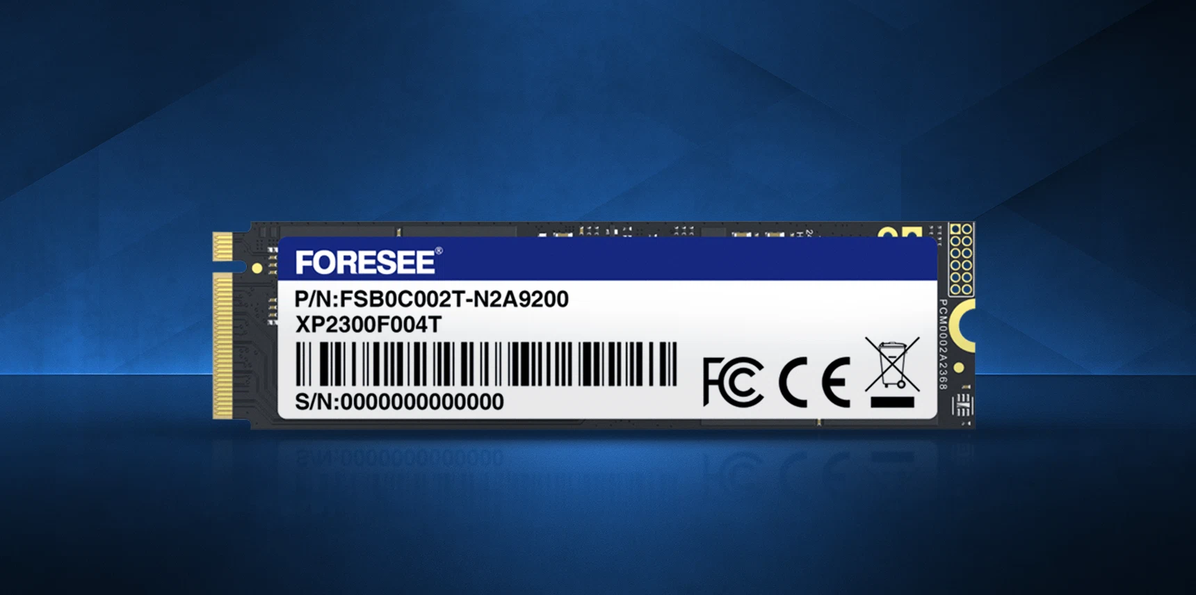
Lexar Enterprise’s FORESEE industrial SSD line addresses the machine vision storage architecture requirements outlined above across multiple form factors and interface configurations. For embedded and industrial applications, see the full Embedded/Industrial solutions page.
FORESEE FM9 Series – NVMe M.2 Industrial SSD
The FM9 series targets high-throughput machine vision applications requiring NVMe performance in the M.2 2280 form factor. Key specifications:
- Interface – PCIe Gen 3 x4 NVMe 1.3
- Sequential write throughput – up to 1800MB/s (capacity-dependent)
- Operating temperature – -40°C to +85°C industrial grade
- Endurance – available in 1DWPD and 3DWPD configurations
- Capacities – 128GB to 1TB
- Power loss protection – capacitor-backed PLP on write buffers
The FM9 series is appropriate for single-camera high-fps applications and multi-camera arrays where aggregate sustained write demand falls in the 800MB/s-1500MB/s range after preprocessing.
FORESEE FS810 Series – SATA Industrial SSD
The FS810 series addresses SATA deployments requiring industrial temperature ratings and verified endurance for continuous write workloads. Relevant specifications:
- Interface – SATA III 6 Gb/s
- Sequential write throughput – up to 520MB/s
- Operating temperature – -40°C to +85°C
- Endurance – up to 3 DWPD in high-endurance configurations
- Capacities – 64GB to 1TB
- Form factors – 2.5-inch and M.2 2280/2242
The FS810 series is well-matched to single-camera systems at 30fps-60fps, 2 to 4 camera configurations with preprocessing pipelines, and retrofit applications where existing platforms use SATA controllers. For engineering sample requests, custom NAND configurations, and compliance documentation, visit the FORESEE Solid-State Drives page.
Machine Vision Storage Architecture Selection Checklist
Use this checklist during component evaluation to verify your machine vision storage architecture is correctly specified for your deployment requirements. Work through it in order – each section’s answers inform the decisions that follow.
Frame Buffer and Throughput
- Calculate peak raw data rate – (resolution in megapixels) x (bit depth / 8) x (fps) = MB/s per camera
- Calculate aggregate array output – per-camera rate x camera count
- Determine effective storage write rate – apply compression ratio and frame retention percentage
- Size system DRAM buffer – buffer must absorb (peak rate – sustained write rate) x maximum burst duration
- Verify preprocessing pipeline – confirm what reduces raw data before storage write
Interface Selection
- Compare effective write rate against SATA limit – if sustained writes exceed 400MB/s, select NVMe
- Evaluate latency sensitivity – applications sensitive to write completion timing should prefer NVMe regardless of throughput
- Check platform constraints – verify available PCIe lanes and M.2 slots on target compute platform
- Account for NVMe thermal budget – confirm enclosure thermal design supports NVMe operating temperatures under load
Endurance Verification
- Calculate daily write volume – effective storage write rate (GB/s) x operational hours per day x 3600
- Apply write amplification factor – multiply daily write volume by 1.5x-3x depending on workload mix
- Calculate required DWPD – (adjusted daily write volume in GB) / (drive capacity in GB)
- Select drive DWPD rating above calculated requirement – minimum 20% margin
- Verify SLC cache behavior – confirm drive performance specification under sustained write conditions beyond SLC cache capacity
- Evaluate pSLC mode – for applications exceeding 2DWPD, assess pSLC-mode drives for endurance margin
Environmental Qualification
- Verify operating temperature range – confirm drive rating covers worst-case enclosure temperature, not just ambient
- Check vibration specification against deployment environment – verify test standard referenced in datasheet
- Confirm shock rating – pay attention to operational shock, not just non-operating shock
- Assess power loss protection requirement – if unexpected power loss is possible, specify drives with capacitor-backed PLP
- Review humidity and conformal coating – required for humid, washdown, or chemically active environments
Supply Chain and Lifecycle
- Confirm component longevity commitment – industrial deployments with 5-10 year lifecycles need vendor lifecycle assurance
- Request NAND change notification policy – NAND die changes can affect endurance and performance characteristics
- Verify certifications – AEC-Q100 for automotive-adjacent applications, IEC 60068 for environmental testing, MTBF figures for reliability modeling
- Obtain qualification samples before production commit – run your actual workload on actual drives under representative thermal conditions before finalizing the BOM
| Key Takeaways for Machine Vision Storage Architecture |
|---|
|
Is Your Machine Vision Storage Architecture Specified Correctly?
Machine vision storage architecture is not a late-stage decision. The choices made at the frame buffer design stage propagate forward through interface selection, endurance specification, and environmental qualification. A system designed with accurate write workload data, correctly sized buffers, and appropriately rated NAND will run through its deployment lifecycle without storage-related failures.
Underspecified storage – whether the failure mode is throughput saturation, NAND endurance consumption, or environmental degradation – creates failures that are difficult to diagnose in the field and expensive to remediate. The specifications exist. The products built to meet them exist. The gap is usually in how thoroughly the workload was characterized before the drive was selected.
If your machine vision project is in the component evaluation stage, Lexar Enterprise’s FORESEE industrial SSD line and technical team are available to support drive selection, workload analysis, and qualification planning. For more on how Lexar Enterprise supports embedded and industrial system designers, visit the Knowledge Center. Request datasheets, compliance documentation, or engineering samples through the Contact Us page.