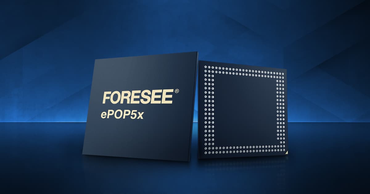
Memory footprint is rarely the first thing locked in a wearable design, but it becomes the constraint that overrides decisions about device thickness and PCB layout. The answer is package-on-package integration – and Lexar Enterprise’s ePOP5x brings it to the 0.6mm thickness threshold that next-generation AI wearables require.
The ePOP5x integrates eMMC 5.1 flash storage and LPDDR4x DRAM into a single package measuring 8mm x 9.5mm with a maximum thickness of just 0.6mm. It ships in two mainstream capacity configurations: 32GB eMMC + 16Gb LPDDR4x and 64GB eMMC + 16Gb LPDDR4x, and it supports LPDDR4x frequencies up to 2133 MHz, or 4267 Mbps data rate. At 0.6mm, the ePOP5x is nearly 25% thinner than its 0.8mm predecessor, the ePOP3/ePOP4 generation. For AI wearable memory design, that 0.2mm reduction is the difference between a watch that meets its thickness target and one that doesn’t.
This is what the wearable paradox looks like in engineering terms: devices need more processing capability, more storage, and more DRAM to run on-device AI models. At the same time, they must also get thinner, lighter, and longer-lasting on a smaller battery. Package-on-package memory is one of the few architectural choices that moves all four variables in the right direction at once.
Wearable Device Memory Constraints and Integration Challenges
A wrist-worn device operates under constraints that don’t exist in any other embedded computing category. Battery volume determines runtime, and it competes directly with every other component for the same internal space. The PCB is not just a routing substrate. In a smartwatch, a PCB is structural. Every square millimeter allocated to memory comes out of the battery area, sensor placement, or the antenna clearance zone on which RF performance depends.
The memory constraint is compounding. First-generation smartwatches ran basic step counting and notifications, which were manageable with 512MB of DRAM and 4GB of storage. An AI wearable running continuous health monitoring with on-device inference, voice assistant processing, and gesture recognition requires 2GB to 4GB of DRAM and 32GB to 64GB of storage simultaneously. That is a 4x to 8x increase in memory requirement for a device whose PCB footprint has not grown.
Discrete components hit a wall at this scale. A standard 11.5mm × 13mm eMMC occupies 149.5mm² of PCB area. Adding a discrete LPDDR4x package brings the combined footprint over 230mm², nearly the entire memory zone of a compact smartwatch PCB, before routing clearance, decoupling capacitors, or EMI management is accounted for.
ePOP5x Architecture: eMMC 5.1 + LPDDR4x Integration
Package-on-package (PoP) technology stacks memory die vertically above the SoC rather than placing components side-by-side on the PCB. The lower package connects to the SoC ball grid array. The upper package, containing flash and DRAM die, stacks directly on top via through-mold vias or stacked BGA interconnects. Memory occupies the SoC footprint rather than the PCB surface area.
The Lexar Enterprise ePOP5x implements this architecture with eMMC 5.1 flash and LPDDR4x DRAM integrated into a single 8mm x 9.5mm package. The eMMC 5.1 layer delivers HS400 sequential read performance of up to 400MB/s and handles the storage workload, including OS images, application data, ML model weights, and user data. The LPDDR4x layer provides the working memory bandwidth that AI inference and real-time sensor fusion require, running at up to 2133MHz (4267Mbps data rate) across dual channels.
The integrated controller supports LDPC error correction across both memory types, maintaining data integrity through the temperature cycling and mechanical stress that wrist-worn devices experience. Lexar Enterprise’s in-house firmware adds sleep mode management and dynamic frequency scaling, both critical for battery life, that a two-component discrete solution would require the host SoC firmware to manage independently.
Ultra-Thin Package Design: 0.6mm vs 0.8mm Predecessor
The 0.6mm maximum thickness of the ePOP5x is not an incremental refinement. Previous ePOP generations used conventional wire-bond die stacking that constrained the minimum package height to 0.8mm – 0.9mm. The ePOP5x achieves 0.6mm through advanced flip-chip bonding and wafer-level thinning of constituent die, reducing individual die thickness until the stacked assembly clears 0.6mm with the overmold included.
The engineering impact for wearable device design is direct. A 0.2mm reduction in memory package height translates to 0.2mm of device thickness that can go toward a larger battery, thinner chassis, or additional sensor integration. In a device category where industrial design teams fight for tenths of a millimeter, this is not a marginal gain.
Wearable PCB Layer Budget: 11mm Device Thickness
Discrete eMMC + LPDDR4x
No thermal clearance remaining
ePOP5x Integrated
Battery gain + thermal clearance retained
Illustrative layer budget for an 11mm smartwatch. The 1.0mm saved by ePOP5x integration can go toward a larger battery or thermal clearance.
Power Consumption Optimization for Battery-Powered Wearables
A typical AI smartwatch uses a battery with a capacity of 250mAh to 420mAh, with a total device power budget of 60mW to 120mW during active use. Memory’s share matters because it is always-on, even when the display is off, and the SoC is in a low-power state, DRAM must maintain self-refresh to preserve working memory contents.
LPDDR4x reduces I/O termination power by roughly 40% compared to standard LPDDR4 at equivalent data rates, operating at 0.6V VDDQ instead of 1.1V for LPDDR4. The ePOP5x’s integrated package reduces this further by eliminating PCB trace routing between discrete eMMC and LPDDR components; shorter signal paths mean lower switching energy per transaction.
AI Wearable Memory Power Budget Analysis
| Memory State | LPDDR4x Power | eMMC 5.1 Power | Total (ePOP5x) | Wearable Scenario |
| Deep sleep | ~0.35mW | ~0.6mW | ~1.0mW | Watch face only, no active sensing |
| Idle / self-refresh | ~1.2mW | ~1.5mW | ~2.7mW | Passive HR monitoring, background sync |
| Active inference | ~8mW | ~5mW | ~13mW | On-device ML model running (DNN inference) |
| Peak burst (boot/OTA) | ~18mW | ~35mW | ~53mW | System boot, app install, firmware update |
Estimated values based on LPDDR4x JEDEC JESD209-4C and eMMC 5.1 JEDEC JESD84-B51 typical operating conditions at VCC 1.8V / 0.6V VDDQ.
Lexar Enterprise’s firmware implements sleep scheduling that coordinates eMMC sleep entry with LPDDR4x self-refresh timing, preventing one component from blocking the other from entering its lowest-power state. In wearables, where memory spends 80% to 90% of its time in idle or sleep, this coordination has a greater impact on daily energy consumption than peak active-mode efficiency.
AI Inference Memory Requirements for Wearable Devices
On-device AI in wearables is not a single workload – it is a stack of concurrently active models with different memory access patterns. A health monitoring platform running today typically includes a heart rate variability model, a step and activity classification model, a sleep stage detection model, and, on premium devices, an ECG arrhythmia screening model. Each model has its own weight file that must be loaded from eMMC to LPDDR4x for inference.
Typical quantized model weight sizes for wearable neural networks range from 2MB to 8MB for HR/HRV monitoring models, 4MB to 15MB for activity classification, 8MB to 25MB for sleep stage detection, and 15MB to 50MB for ECG arrhythmia screening. Running three to four models simultaneously requires 30MB to 100MB of DRAM working memory for weights plus activation buffers. The ePOP5x’s 16Gb (2GB) LPDDR4x provides the working memory capacity for this concurrent inference stack with margin for the OS and middleware. The 32GB or 64GB eMMC holds the full model library, training logs, and the health history database that personalization algorithms reference during inference.
SoC Compatibility and PoP Mounting Advantages
PoP mounting means the ePOP5x connects directly to the wearable SoC’s memory interface balls rather than routing through PCB traces to distant component pads. For LPDDR4x at 4267Mbps, trace routing of 20mm-30mm between a discrete package and the SoC requires impedance-controlled differential routing, which consumes PCB layers. PoP eliminates this routing; the LPDDR4x connection is the stacked package interface, measured in hundreds of micrometers rather than centimeters.
Qualcomm’s Snapdragon Wear 4100+ and MediaTek’s MT6835 wearable SoC both support PoP LPDDR4x memory interfaces. The ePOP5x’s 8mm x 9.5mm footprint is compatible with both platforms’ memory interface ball patterns, with Lexar Enterprise offering customized configurations for specific SoC PoP interface requirements. The eMMC 5.1 connection routes through standard HS400 signals that both platforms support without modification to the host memory controller configuration.
PCB Space Savings and Form Factor Design Flexibility
The quantified comparison is clear. A standard eMMC 11.5mm x 13mm package plus a discrete 9mm x 9mm LPDDR4x package requires approximately 230mm² of PCB area before routing clearance. The ePOP5x at 8mm x 9.5mm occupies 76mm², a 67% reduction.
That recovered area gives wearable PCB designers three options depending on the device’s primary constraint:
- Battery capacity increase: 150mm² of recovered PCB area translates to roughly 50 to 80 mAh of additional battery capacity in a stacked battery configuration – a 15% to 25% runtime improvement on a typical smartwatch battery
- Additional sensor integration: PPG sensors (green + infrared + red LED arrays), SpO2 sensors, skin conductance sensors, and barometric pressure sensors each require 10mm to 25mm² of PCB area; the recovered memory footprint fits three to five additional sensor ICs
- Thinner device chassis: With ePOP vertical stacking reducing memory height to 0.6mm versus 1.6mm for stacked discrete components, the saved 1.0mm vertical space can reduce device thickness by the same amount without changing battery capacity
Application Examples: Smart Watches, Hearables, Medical Wearables
Smart watches are the primary application. The 64GB + 16Gb configuration handles health data history, offline media, and on-device AI model weights simultaneously. Lexar Enterprise’s firmware targets a sub-2-second cold boot time to the watch face display, meeting user expectations for always-available wrist-worn devices.
Hearables – AI-powered earbuds and hearing aids – operate under even tighter PCB constraints. True wireless earbud PCBs range from 100 mm² to 200 mm² total. The ePOP5x’s 76 mm² footprint is viable for premium hearable designs running local voice processing and active noise cancellation ML models, with the 32GB + 16Gb configuration covering voice assistant firmware with margin.
Medical wearables, including continuous glucose monitors, cardiac rhythm monitors, and fall-detection patches, have distinct constraint profiles. The LDPC-protected integrated controller and Lexar Enterprise’s -25°C to +85°C operating range cover both the skin-contact temperature profile and the data integrity requirements that body-worn medical devices demand.
Selecting ePOP vs Discrete Components: A Design Decision Guide
ePOP integration is the right choice when at least two of these conditions apply:
- PCB footprint is constrained below 200mm² for the memory zone – typical of smartwatches, hearables, and compact medical patches
- The device thickness target is under 12mm, where every 0.1mm reduction requires engineering justification
- Battery capacity is already at a minimum for the target runtime, and the recovered PCB area can be converted to battery volume
- AI inference workloads require 1GB to 2GB DRAM alongside 32GB to 64GB persistent storage
- Single-source memory qualification simplifies the supply chain and reduces BOM complexity
Discrete components remain appropriate when PCB space is unconstrained, when DRAM requirements exceed the ePOP5x’s 16Gb (2GB) ceiling, or when storage needs exceed 64GB.
For the AI wearable memory design problems that define new smartwatch, hearable, and medical wearable programs – devices that need more capability in less space – the ePOP5x resolves the constraint that discrete component approaches cannot.
Contact Lexar Enterprise to request the ePOP5x product brief, PoP mounting specifications for your target SoC, and sampling for your wearable development program.