AR device memory requirements differ fundamentally from those of smartphone or tablet memory designs. The processing pipeline for smart glasses runs image capture, preprocessing, AI inference, AR overlay compositing, and display output in a continuous loop – all within a 5W power budget on a device that cannot exceed 100g. Every memory access either contributes to immersive AR or degrades it.
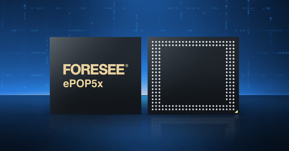
The ePOP5X architecture addresses this directly. By integrating eMMC 5.1 flash storage and LPDDR5 DRAM into a single 0.6mm package-on-package structure, ePOP5X eliminates signal routing overhead between discrete components, reduces the PCB footprint that AR processor boards often cannot afford, and keeps the combined memory subsystem within the power envelope required by glasses form factors. For AR device designers working with Qualcomm Snapdragon AR platforms and similar processors, this integration changes what’s possible within the physical constraints of a frame-mounted compute module.
Smart Glasses and AR Device Memory Architecture Challenges
The AR device design space sits at an intersection of constraints that exist nowhere else in consumer electronics. Head-worn devices must simultaneously satisfy requirements that typically trade off against each other in conventional product design.
The primary constraints driving AR memory architecture decisions include:
- Weight budget: Consumer smart glasses target under 100g total. The compute module, including processor, memory, wireless silicon, and optics driver, typically gets 15g-25g of that budget. Discrete memory configurations add mass through additional package count, PCB area, and the copper pour required for signal routing
- Thermal ceiling: Surface temperature limits of 38°C-40°C at temples and nose bridge restrict total device power dissipation. Without active cooling, every milliwatt of memory idle power accumulates as heat in a thermally compact enclosure
- Power envelope: A 5W total device budget shared across optics, wireless, compute, and memory leaves under 1W for the memory subsystem during sustained AR operation
- PCB area: Glasses arms and bridge sections offer PCB zones with widths of 8mm-15mm. The memory layout must fit within these narrow corridors while maintaining signal integrity at LPDDR5 speeds
- Latency sensitivity: AR overlay misalignment exceeding 20ms creates perceptible visual artifacts. Memory-induced latency anywhere in the pipeline directly degrades the AR experience in ways users notice immediately
Discrete eMMC plus LPDDR configurations fail on multiple dimensions here. They consume more PCB area, generate more heat through longer signal paths, and require more complex board layouts, which increase manufacturing costs in the low-volume production runs typical of AR device development cycles.
Real-Time Image Processing and Low-Latency Requirements
The AR processing pipeline has a memory access pattern unlike any other embedded application. Each frame cycle, occurring 30 to 90 times per second depending on device class, requires the processor to read raw image data from camera buffers, load preprocessing parameters, run inference against a model in working memory, composite overlay elements, and push the result to the display driver. That’s four to six distinct memory operations per frame, each with latency requirements measured in microseconds.
At 60fps, the total frame budget is 16.7ms. Breaking that budget down by pipeline stage shows where memory bandwidth and latency matter most:
- Image capture and buffer transfer (2ms-3ms): Camera frame data is moved from the sensor to the DRAM frame buffer. Memory bandwidth determines how quickly full-resolution frames clear the capture pipeline
- Preprocessing (1ms-2ms): Distortion correction, white balance, and image normalization require read-modify-write operations against the frame buffer
- AI inference (5ms-8ms): Object recognition, depth estimation, and scene understanding models run from DRAM. Model weights must be resident in working memory – any cache miss that triggers an eMMC load adds unacceptable latency mid-frame
- Overlay compositing (2ms-3ms): AR graphics elements composite against the processed camera frame. This stage is memory-bandwidth-bound, requiring simultaneous read of camera data and write of composite output
- Display output (1ms-2ms): Composite frame transfers to the display buffer for optical rendering
At LPDDR5’s 4267 Mbps data rate, the ePOP5X’s DRAM subsystem can sustain approximately 533MB/s. A 1080p camera frame at 24-bit color is roughly 6MB. At 60fps, camera throughput alone requires about 360MB/s of sustained bandwidth – leaving headroom for concurrent inference and compositing operations, but only if the memory architecture is tight. Discrete LPDDR with longer signal paths loses a measurable percentage of that bandwidth to routing overhead. Integrated PoP recovers it.
AI Inference Memory Bandwidth for AR Applications
On-device AI inference in AR applications is fundamentally a memory-bandwidth problem. The compute operations themselves – matrix multiplications, convolutions, attention mechanisms – execute quickly on the neural processing units built into modern AR processors. What limits inference speed in practice is how fast model weights move from memory into the NPU’s compute units.
AR inference models vary significantly in size and memory access patterns by application type:
- Object recognition and labeling: 5MB-25MB models, accessed sequentially per inference pass. Fits comfortably in LPDDR5 working memory; requires fast initial load from eMMC on app launch
- Hand tracking and gesture recognition: 2MB-8MB models, accessed at high frequency for low-latency gesture response. Must remain resident in DRAM during active use – cannot tolerate mid-session eMMC reload
- Scene understanding and spatial mapping: 40MB-120MB models with irregular access patterns. The larger end of this range stresses 2GB DRAM configurations and requires careful model management to prevent working memory pressure
- Face recognition and social AR features: 10MB-50MB models. Intermittent inference triggered by detection events, but latency requirements are tight enough that cold-start model loading from eMMC is perceptible
The ePOP5X’s LPDDR5 at 4267Mbps provides the bandwidth to keep multiple moderate-size models resident simultaneously, allowing AR applications to switch inference contexts, from object recognition to gesture tracking to face analysis, without reloading from storage. That resident-model capability is what separates responsive AR from AR that stutters when the scene changes.
ePOP5X Integration: eMMC Storage and LPDDR5 DRAM Benefits
Package-on-package integration in ePOP5X isn’t just a board space optimization. The architectural benefits extend to signal integrity, thermal behavior, and manufacturing yield, specifically for AR device production.
Signal integrity at LPDDR5 speeds requires controlled impedance traces with tight length matching between data lines. In a discrete configuration, those traces route across the PCB surface for 5mm-15mm between the LPDDR package and the processor. On a narrow glasses arm PCB, maintaining consistent impedance over that distance is difficult – via transitions, nearby copper pours from power delivery, and the mechanical flex of glasses frames all introduce variability that manifests as signal integrity margin loss.
The ePOP5X PoP interface moves those high-speed connections into the package stack, where they’re controlled by the package substrate design rather than PCB layout. The result is consistent signal quality independent of PCB routing quality, leading to a significant yield improvement for the narrow-board layouts that AR devices require.
Capacity configurations for AR applications map to distinct device tiers:
- 32GB eMMC + 2GB LPDDR5: Enterprise AR glasses for single-application use cases – warehouse picking, maintenance guidance, remote expert assist. The 2GB DRAM headroom supports one primary inference model resident, plus OS and application working sets
- 64GB eMMC + 2GB LPDDR5: Consumer smart glasses with broader application ecosystems. The additional storage supports multiple AI model libraries, richer content caching, and the larger firmware footprints that multi-function AR devices require
Power Budget Constraints in Glasses Form Factors
A 5W total device power budget for smart glasses breaks down roughly as follows across major subsystems – though specific allocations vary by device architecture:
- Application processor and NPU: 1.5W-2.5W during active AR inference
- Display and optical engine: 0.8W-1.5W, depending on brightness and waveguide technology
- Wireless (Wi-Fi 6, Bluetooth): 0.3W-0.6W during active connectivity
- Camera and ISP: 0.2W-0.4W during active capture
- Memory subsystem: 0.2W-0.5W target across DRAM and storage
LPDDR5’s power architecture was designed for exactly this class of constraint. The standard includes multiple power-down modes that AR devices can exploit based on pipeline state. During display-on AR rendering, when the processor is active, but memory access is bursty rather than continuous, LPDDR5 self-refresh modes reduce DRAM power to under 50 mW between bursts. When the user removes the glasses and the device enters standby, deep power-down reduces DRAM current to the microamp range while retaining state.
eMMC 5.1’s contribution to power budget management is its near-zero idle consumption. Storage access in AR applications is infrequent during active operation, models are loaded at session start, and OS data is cached in DRAM. The eMMC component draws less than 1 mW when inactive, making its contribution to the sustained power budget negligible.
Thermal Management in Head-Worn Devices
The 40°C surface temperature limit for head-worn devices isn’t arbitrary; it’s the threshold above which skin contact becomes uncomfortable and potentially harmful during extended wear. AR glasses that exceed this limit generate user complaints, return events, and regulatory attention in medical device categories.
Thermal management in glasses starts with minimizing heat generation at the component level, since the heat-rejection options available in glass form factors are limited. There’s no space for a heatsink. Vapor chambers don’t fit in a 4 mm-thick glass arm. Thermal design relies on spreading heat across the enclosure surface area and conducting it away from hotspots through the frame structure.
The ePOP5X integration reduces thermal load on the memory subsystem through two mechanisms:
- Reduced I/O power: Shorter signal paths in the PoP stack consume less drive current than long PCB traces, directly reducing heat generation at the processor I/O pads
- Single thermal source: Consolidated memory heat generation in one package location simplifies thermal spreading design compared to managing two discrete memory hotspots at different board locations
Designers targeting sub-38°C surface temperatures should budget the ePOP5X package at 200mW-350mW thermal dissipation during sustained AR operation, with thermal resistance to ambient depending on enclosure material and contact area with the frame structure. Magnesium alloy frames conduct heat more effectively than injection-molded polymer, a design choice that directly affects how aggressively the memory subsystem can operate before surface temperature limits are reached.
Application Processor Integration: Qualcomm AR Platforms
Qualcomm’s Snapdragon AR platform series defines the reference architecture for most current smart glasses designs. Its memory subsystem expects LPDDR5 via PoP attachment, which aligns directly with ePOP5X’s integration model. Adapting to discrete LPDDR memory on a PoP platform requires additional signal integrity validation, which integrated ePOP5X avoids entirely.
The eMMC 5.1 interface connects via HS400 protocol, natively supported by Snapdragon AR platforms, delivering up to 400MB/s sequential read for OS boot, app launch, and on-demand model loading without becoming a pipeline bottleneck.
Integration validation should include thermal characterization under sustained inference workloads, signal integrity margin testing at temperature extremes, and power consumption verification across LPDDR5 power states. Lexar Enterprise provides application notes and reference designs for ePOP5X integration with common AR processor platforms.
Future Outlook: Metaverse and Spatial Computing Requirements
Current AR glasses represent the early architecture of a device category that will evolve substantially over the next several hardware generations. Memory demand grows along a clear trajectory:
- Higher display resolution: Moving from 720p to 1080p per eye doubles frame buffer memory requirements; 4K per eye increases it by 8x
- More simultaneous AI models: Object recognition, user intent prediction, and real-time translation running concurrently multiply DRAM residency requirements
- Spatial mapping persistence: Persistent AR anchors require larger on-device storage for map data across sessions
- Multi-user AR: Shared experiences require faster storage access for environment synchronization
For enterprise AR glasses that require sustained single-application performance, the 32GB+2GB ePOP5X configuration supports current-generation AR workloads. For consumer smart glasses targeting broader application ecosystems, the 64GB+2GB configuration supports the model library depth and content storage that differentiates a capable AR experience from a constrained one.
If your AR device project is hitting the memory bottleneck – latency spikes, thermal limits, or PCB layout constraints that discrete memory can’t resolve within your form factor – contact the Lexar Enterprise technical team to discuss ePOP5X integration with your target AR processor platform and validate the configuration against your specific performance and thermal requirements.