Overview

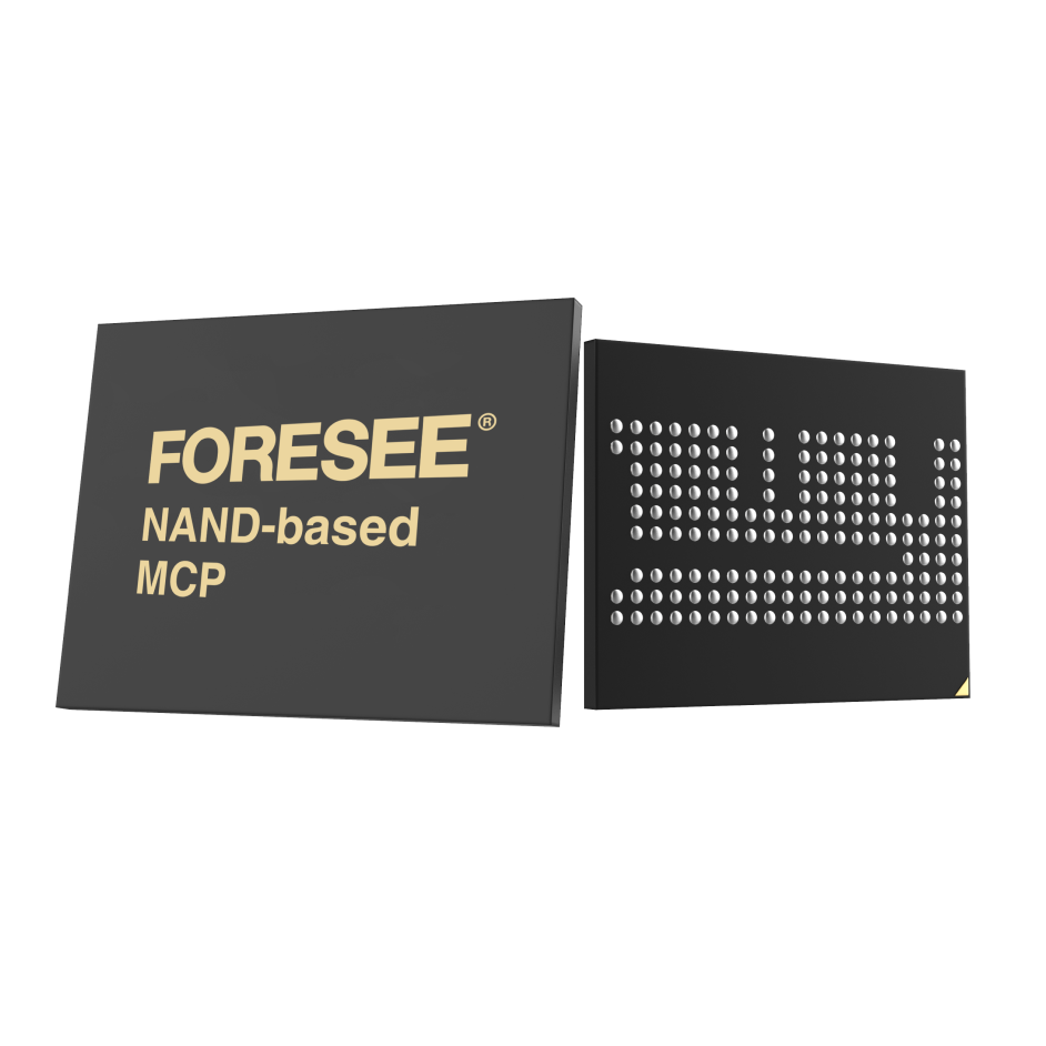
NAND-based MCP
NAND-based MCP
A boot code source and DRAM in a single package to improve board space savings and optimize layout. Want to learn more about this product? Our sales team is ready to help.
Specifications
LPDDR2 NAND-based MCP
Capacity (Size)
Part Number
Request Sample
Applications

Mobile Phones

4G/5G Wireless Modules

Digital Cameras

Internet of Things (IoT) Devices

Laptop Computers
Key Benefits
An All-in-one Chip
SLC and LPDDR DRAM multi-chip package memory provides two-die in one package, delivering an all-in-one solution to support an optimized interface.
Fits in Tight Spaces
A minimal package footprint routes signals to a single component to provide an easier, efficient package footprint that provides excellent PCB space savings.

Optimized Power Efficiency
10mA is typical data for all the SLC NAND in the market, it couldn’t be taken as special/optimized feature.