Embedded memory selection starts with application requirements rather than technology features. Your engineering team should define five critical parameters before evaluating specific memory architectures:
- Bandwidth requirements: Sequential throughput (MB/s) and random access performance (IOPS) determine whether applications need high-speed DRAM or storage-focused NAND solutions
- Power budget allocation: Active operation consumption, standby mode draw, and deep power-down capabilities affect battery life and thermal management
- Temperature grade specifications: Commercial (0°C to 70°C), industrial (-40°C to 85°C), and automotive (-40°C to 125°C) grades define environmental operating ranges
- Form factor constraints: PCB area limitations, package height restrictions, and integration complexity influence technology selection
- Cost-per-GB targets: Budget allocations differ significantly between DRAM (higher cost, volatile) and NAND storage (lower cost, non-volatile)
This requirement-driven framework prevents common selection errors, like choosing high-bandwidth LPDDR5 for applications requiring non-volatile storage, or specifying industrial-grade eMMC when automotive temperature qualifications are mandatory.
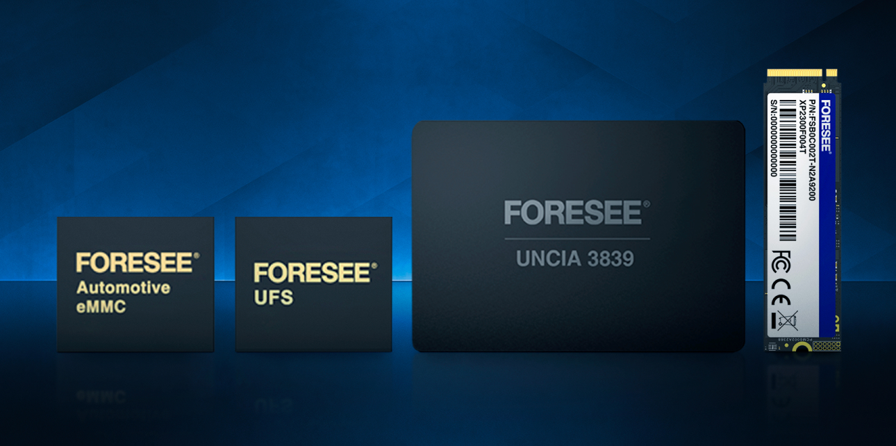
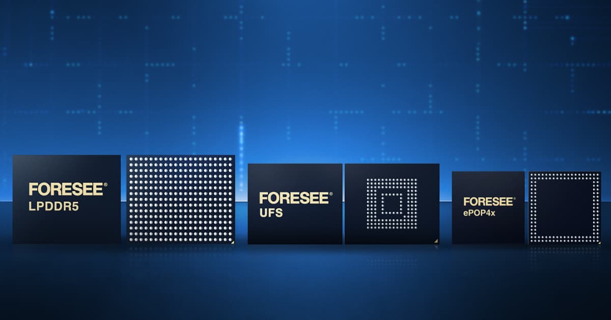
Embedded memory technologies fall into three distinct architecture categories. LPDDR5 and LPDDR5X provide volatile DRAM with bandwidth reaching 51.2 GB/s for processor-intensive applications. UFS 4.0 and eMMC 5.1 deliver non-volatile NAND storage with sequential read speeds up to 4200MB/s for data retention. ePOP solutions integrate both DRAM and storage in single packages optimized for space-constrained designs.
Understanding Embedded Memory Architecture Categories
DRAM solutions including LPDDR5 and LPDDR5X provide volatile memory requiring continuous power to maintain data. These architectures excel in applications demanding low-latency random access and sustained high bandwidth — characteristics that make LPDDR ideal for processors, GPUs, and AI accelerators. JEDEC LPDDR5 specifications define transfer rates from 4266MT/s to 6400MT/s, delivering up to 51.2GB/s bandwidth in x32 configurations.
The volatility trade-off means LPDDR solutions lose data during power cycles, requiring non-volatile storage for firmware and persistent data. This architectural limitation explains why most embedded systems pair LPDDR DRAM with separate NAND storage.
NAND storage solutions including UFS and eMMC provide non-volatile memory retaining data without power. UFS 4.0 delivers sequential read performance up to 4200MB/s with command queue depths supporting multiple concurrent operations. eMMC 5.1 offers lower-cost storage with sequential performance reaching 400MB/s, sufficient for firmware storage and moderate data requirements.
Integrated ePOP solutions combine LPDDR DRAM and UFS storage in single packages, stacking memory dies vertically to minimize PCB footprint. ePOP5X configurations pair LPDDR5 DRAM with UFS 3.1 storage, providing both high-bandwidth volatile memory and non-volatile storage in packages measuring 11.5mm x 13mm, roughly 60% smaller than discrete implementations.
The integration benefits come with thermal management challenges. Stacked configurations concentrate power dissipation in smaller volumes, potentially creating hot spots exceeding individual component ratings. ePOP thermal design requires analysis of junction temperatures under sustained workloads, particularly in automotive applications where ambient temperatures reach 85°C to 105°C.
Application Requirements Framework for Memory Selection
Bandwidth requirements analysis begins with workload characterization, primarily with stress storage subsystems. UFS 4.0 sequential read performance reaching 4200MB/s supports 4K video capture at 120fps. eMMC 5.1 sequential write speeds around 250MB/s handle 1080p video or moderate sensor data rates.
Random access patterns that are typical in operating system operations and database queries benefit from LPDDR DRAM’s sub-10ns latency compared to NAND storage latencies measured in microseconds. Mobile edge AI applications processing camera frames require LPDDR5 bandwidth for neural network inference, while automotive ADAS systems running object detection algorithms demand LPDDR5X performance.
Power budget allocation affects technology selection across active, standby, and deep power-down modes. LPDDR5 active power ranges from 50mW to 200mW per GB depending on access patterns. Self-refresh modes reduce consumption to 5mW to 15mW per GB, while deep power-down reaches sub-1mW levels – critical for battery-powered IoT devices.
Form factor constraints become critical in wearables, compact IoT devices, and automotive applications with limited PCB area. Discrete LPDDR5 packages in package-on-package (PoP) configurations stack directly on application processors, minimizing routing length. Standard BGA packages require dedicated PCB real estate but simplify thermal management.
LPDDR5 and LPDDR5X DRAM Solutions Overview
LPDDR5 architecture defined in JEDEC JESD209-5 specification delivers bandwidth improvements over LPDDR4X through higher transfer rates (up to 6400MT/s vs4266 MT/s) and architectural enhancements. A x32 LPDDR5-6400 configuration provides 51.2GB/s theoretical bandwidth, which should be sufficient for processors running multiple AI models, graphics rendering, or video processing workloads simultaneously.
Power efficiency gains come from voltage optimization and duty cycle improvements. LPDDR5 operates at 1.05V VDDQ and 1.8V VDD2, but improved I/O design delivers 20% to 30% lower power consumption at equivalent bandwidth compared to LPDDR4X. Deep sleep modes including self-refresh and power-down states enable battery-powered devices to maintain DRAM content while minimizing standby current.
LPDDR5X extensions push transfer rates to 8533MT/s, delivering 68.3GB/s bandwidth in x32 configurations. These extreme-performance variants target automotive systems requiring maximum memory bandwidth, such as applications for real-time 3D mapping, multi-camera fusion processing, or large language model inference on edge devices.
Typical LPDDR5 applications include automotive ADAS processors requiring low-latency access to sensor fusion algorithms, mobile edge AI platforms running computer vision models, and high-performance industrial controllers. Package options include 6GB to 16GB densities in both PoP and discrete BGA formats, with automotive-grade versions qualified to AEC-Q100 Grade 2 (-40°C to 105°C) or Grade 3 (-40°C to 125°C) specifications.
UFS and eMMC NAND Storage Solutions Overview
UFS 4.0 architecture represents the current performance tier for embedded NAND storage, delivering sequential read speeds up to 4200MB/s and write performance reaching 4000MB/s, which is approximately 10x faster than eMMC 5.1 solutions. The performance advantage comes from full-duplex differential signaling using dedicated read and write lanes, compared to eMMC’s half-duplex shared data bus.
Command queue depth represents another critical UFS advantage. UFS supports 32 outstanding commands through SCSI-based command sets, allowing storage controllers to optimize operation scheduling. eMMC command queuing supports only two prioritization levels, limiting performance optimization in complex workloads.
UFS 3.1 maintains mainstream adoption across automotive and industrial applications requiring reliable performance without UFS 4.0 power consumption. Sequential read performance reaches 2900MB/s with write speeds around 1200MB/s are sufficient for automotive infotainment systems, industrial vision inspection, and edge computing gateways.
eMMC 5.1 continues serving cost-sensitive applications where sequential performance requirements stay below 400MB/s read and 250MB/s write. IoT devices storing configuration data, industrial controllers logging periodic sensor readings, and entry-tier automotive systems benefit from eMMC’s lower cost-per-GB while accepting reduced performance.
ePOP Integrated Memory Solutions Overview
ePOP5X architecture integrates LPDDR5 DRAM and UFS 3.1 storage in vertically-stacked packages optimizing PCB area for space-constrained applications. Typical configurations pair 4GB to 8GB LPDDR5 with 64GB to 256GB UFS storage in 11.5mm x 13mm packages – delivering complete memory subsystems in roughly 150mm² footprint.
Form factor advantages become critical in wearable devices, compact IoT sensors, and mobile accessories where PCB area directly impacts product size. Smartwatches, fitness trackers, wireless earbuds, and compact camera modules benefit from ePOP integration reducing memory subsystem footprint by 60% compared to discrete implementations.
Thermal management considerations require analysis in ePOP designs. Stacked configurations place DRAM and storage dies in close proximity, concentrating power dissipation. Junction temperatures under sustained workloads may exceed individual component ratings even when package surface temperatures appear acceptable.
Memory Selection Decision Framework
Step 1 – Define application bandwidth requirements by characterizing workload patterns. Calculate sequential throughput needed for video capture or data logging. Measure random access requirements for operating system operations. Sequential workloads above 1000MB/s indicate UFS 3.1 or UFS 4.0 requirements. Random access patterns requiring sub-microsecond latency need LPDDR5 DRAM.
Step 2 – Establish power budget constraints across operating modes. Measure active consumption during peak workloads, standby current during idle periods, and deep sleep requirements. LPDDR5 self-refresh modes consuming 5mW to 15mW per GB suit applications with frequent DRAM access. UFS power gating below 5mW benefits intermittent storage applications.
Step 3 – Determine temperature grade requirements based on deployment environments. Commercial-grade components (0°C to 70°C) serve indoor consumer electronics. Industrial-grade solutions (-40°C to 85°C) support factory automation and outdoor IoT. Automotive-grade memories (-40°C to 125°C per AEC-Q100 Grade 3) are mandatory for engine zone installations.
Step 4 – Evaluate form factor and PCB area constraints. Measure available board space for memory components. PoP configurations minimize routing length but require application processor compatibility. Discrete packages offer flexibility but consume more PCB area. ePOP solutions optimize footprint at the cost of thermal headroom.
Step 5 – Consider cost-per-GB targets within system budget allocations. LPDDR5 typically costs $8 to $15 per GB depending on density and automotive qualification. UFS storage ranges from $0.30 to $0.80 per GB based on capacity and performance tier. eMMC provides $0.15 to $0.40 per GB for cost-sensitive applications.
Real-World Application Examples
Automotive telematics control units typically implement UFS 3.1 storage for firmware and maps combined with LPDDR4X DRAM supporting embedded Linux. UFS selection provides sequential write performance handling continuous GPS logging while meeting automotive temperature requirements. 64GB to 128GB UFS capacity stores offline map data. 2GB to 4GB LPDDR4X supports operating system requirements without LPDDR5 cost premium.
Industrial IoT gateways collecting sensor data often pair eMMC 5.1 storage with LPDDR4X DRAM, optimizing cost while maintaining adequate performance. eMMC sequential write speeds around 250MB/s handle typical industrial sensor data rates below 100MB/s aggregate. 32GB eMMC stores historical data for local analysis before cloud upload.
Mobile edge AI platforms running computer vision models require LPDDR5X DRAM providing bandwidth for neural network inference. A typical configuration uses 8GB to 12GB LPDDR5X-8533 delivering 68.3 GB/s bandwidth supporting real-time object detection and multi-camera fusion.
Wearable fitness trackers leverage ePOP5X integration combining 4GB LPDDR5 with 64GB UFS 3.1 in space-constrained designs. The integrated package reduces PCB footprint enabling sleeker industrial design while providing sufficient DRAM and adequate storage for firmware and cached health metrics.
Supplier Qualification and Long-Term Availability
Automotive-grade qualification requirements follow AEC-Q100 standards defining stress testing and reliability validation. Grade 2 qualification (-40°C to 105°C) suits passenger compartment installations. Grade 3 qualification (-40°C to 125°C) is mandatory for engine compartment and safety-critical ADAS applications. Qualification timelines typically require 12 to 18 months.
Product lifecycle expectations differ significantly between consumer and automotive markets. Consumer memory products typically maintain 3 to 5 year availability. Automotive suppliers commit to minimum 10-year production runs with 15-year extended availability for aftermarket support. Industrial applications require 7 to 10 year lifecycles matching equipment service intervals.
Second-source strategies protect against supply disruptions. OEM procurement teams should identify alternative suppliers offering compatible specifications during design phases. JEDEC-standard interfaces like LPDDR5, UFS, and eMMC facilitate second-sourcing compared to proprietary memory architectures.
Embedded memory selection requires systematic evaluation of application requirements against technology capabilities. LPDDR5 and LPDDR5X DRAM serve high-bandwidth applications requiring low-latency access. UFS and eMMC provide non-volatile storage with different performance tiers. ePOP solutions integrate both architectures for space-constrained designs accepting thermal trade-offs.
Your engineering team should begin memory selection by defining bandwidth, power, temperature, and form factor requirements – then evaluate technology options meeting those specifications rather than starting with memory architecture and forcing application fit.