Your design requires storage that won’t fail at -40°C, survive 100,000 write cycles, and meet AEC-Q100 qualification. General-purpose flash won’t cut it. I’ve seen engineering teams lose months of validation time specifying the wrong NAND type for mission-critical applications – choosing TLC for a high-write automotive ECU, or overlooking endurance ratings on industrial IoT nodes that log data continuously.
NAND flash memory is the foundational storage technology behind every industrial SSD, embedded UFS module, and eMMC component in your BOM. Getting the spec right the first time means understanding how NAND flash works at the architecture level – not just the marketing summary.
This guide covers NAND flash memory from cell-level architecture through automotive-grade qualifications, endurance calculations, and interface selection. Whether you’re specifying components for ADAS systems, IIoT edge nodes, or defense-grade storage, this is the technical reference you need before committing to a supplier.
What Is NAND Flash Memory?
NAND flash memory is a type of non-volatile storage that retains data without continuous power. The “NAND” name comes from the logical NAND gate structure used to connect memory cells in series – a design choice that prioritizes storage density over random access speed, making NAND ideal for bulk data storage applications.
Unlike DRAM, which loses data the moment power is removed, NAND flash holds data by trapping electrons in a floating-gate transistor or charge-trap layer. This physical charge state represents stored bits – and it persists through power cycles, making NAND the backbone of every SSD, eMMC module, and UFS component in industrial and automotive systems today.
The key technical distinction engineers should understand is how NAND compares to NOR flash. NOR flash allows random access at the byte level and executes code in-place (XIP), making it suitable for small bootloaders and firmware storage. NAND flash uses page-level access with block erasure, delivering far higher storage density and write throughput. For applications requiring gigabytes of storage – data logging, OS images, media, sensor archives – NAND is the correct architecture.
NAND Flash Cell Types: SLC, MLC, TLC, and QLC Compared
The number of bits stored per cell defines the most critical performance and endurance tradeoffs in NAND flash specification. Each cell type represents a fundamentally different reliability profile, and selecting the wrong type for your write workload is one of the most common sourcing mistakes in embedded system design.
| NAND Type | Bits per Cell | P/E Cycles (Typical) | Relative Speed | Relative Cost | Best Application |
|---|---|---|---|---|---|
| SLC | 1 | 50,000 – 100,000 | Fastest | Highest | Automotive ECU, industrial control, military |
| MLC | 2 | 3,000 – 10,000 | Fast | Moderate | Industrial SSD, embedded computing |
| TLC | 3 | 300 – 1,000 | Moderate | Lower | Read-heavy IIoT, surveillance, HMI storage |
| QLC | 4 | 100 – 300 | Slowest | Lowest | High-capacity, low-write archival storage |
SLC NAND flash memory stores one bit per cell by programming the floating gate to one of two voltage states. This binary simplicity is what gives SLC its exceptional endurance – most SLC NAND is rated for 50,000 to 100,000 program/erase (P/E) cycles, compared to a few hundred for QLC. For automotive-grade applications that must operate across a 15-year vehicle lifespan under continuous write workloads, SLC remains the specification of choice despite its cost premium.
MLC NAND stores two bits per cell using four distinct voltage states. The tighter voltage margins require more sophisticated error correction but deliver a cost-per-bit reduction that makes MLC attractive for industrial SSDs where both endurance and budget matter. Industrial MLC is rated at 3,000 to 10,000 P/E cycles depending on the manufacturer and process node.
TLC and QLC NAND push density further by encoding three or four bits per cell. The tradeoff is significant – each additional bit level narrows the voltage margins between states, increasing the bit error rate and reducing endurance. For read-dominant applications like in-vehicle infotainment content storage or surveillance archive drives, TLC and QLC deliver excellent capacity at competitive cost. For write-intensive applications, they require careful wear leveling and over-provisioning to maintain acceptable lifespan.
pSLC Mode: SLC Performance from MLC or TLC NAND
Pseudo-SLC (pSLC) mode allows MLC or TLC NAND flash to operate with SLC-level reliability by using only one bit per cell during programming. The controller writes to a designated pSLC cache region – sacrificing storage capacity in exchange for dramatically improved endurance and write speed.
For industrial embedded storage applications where full SLC pricing is prohibitive but TLC endurance is insufficient, pSLC mode offers a middle path. A TLC NAND running in pSLC mode can achieve endurance ratings of 30,000 P/E cycles or higher – well above standard TLC limits – while maintaining lower base cost than native SLC silicon.
Engineers specifying eMMC or UFS components for automotive or IIoT applications should confirm whether pSLC mode is supported by the controller and what the effective capacity reduction is. A 128GB TLC eMMC running in full pSLC mode delivers roughly one-third of its rated capacity, a tradeoff that must be accounted for in BOM planning.
NAND Flash Memory Architecture: How It Works
Understanding NAND flash memory architecture explains both its performance advantages and its operational constraints. Every read, write, and erase operation follows the hierarchical structure of the NAND array – and every limitation engineers encounter traces back to this physical organization.
The core architectural units of NAND flash are:
- Cell: The fundamental storage element, a floating-gate or charge-trap transistor that stores charge representing one or more bits of data.
- String: A series of cells connected in series between a bitline and the common source line. The NAND string structure (cells connected like a logical NAND gate) is where the technology gets its name.
- Page: The smallest unit that can be read or written. Page sizes in modern NAND typically range from 4KB to 64KB depending on the generation and manufacturer.
- Block: The smallest unit that can be erased, composed of multiple pages. Block sizes range from 256KB to several megabytes. Crucially, NAND must erase at the block level before rewriting – data cannot be overwritten in place.
- Plane: A group of blocks that can be accessed simultaneously to enable parallel operations, improving throughput.
- Die: A single NAND chip containing multiple planes. Multiple dies can be stacked in a single package for higher capacity.
The write-before-erase constraint is the most operationally significant characteristic of NAND flash. When a page contains valid data that needs updating, the controller must copy the entire block to a buffer, erase the original block, and rewrite the modified data. This process – called garbage collection – is managed by the SSD or eMMC controller’s firmware and is why over-provisioning (reserving a percentage of NAND capacity for controller operations) matters for sustained write performance in industrial applications.
3D NAND Flash Memory: Architecture and Industrial Relevance
Traditional planar (2D) NAND arranges all memory cells on a single layer. As lithography processes push cell dimensions below 20nm, interference between adjacent cells increases, degrading data retention and endurance. 3D NAND flash memory resolves this by stacking cell layers vertically – 64, 96, 128, 176, or more layers depending on the generation – rather than continuing to shrink individual cells.
The industrial relevance of 3D NAND is significant for several reasons:
- Higher density at controlled cost: Stacking layers increases capacity per die without requiring further lithographic shrinkage, improving cost-per-bit economics across the product lineup.
- Improved cell geometry: Larger cell dimensions at the same total die area reduce the electric field interference that plagued late-generation 2D NAND, improving data retention characteristics.
- Extended endurance profiles: Some 3D TLC NAND achieves endurance ratings that exceed those of earlier-generation 2D MLC NAND, narrowing the reliability gap at lower cost points.
- Temperature performance: Industrial-grade 3D NAND is qualified across extended temperature ranges (-40°C to 85°C or higher) suitable for automotive and outdoor industrial deployments.
Lexar Enterprise’s FORESEE-branded industrial storage products are built on 3D NAND architectures, qualified for extended temperature operation and the long-lifecycle availability requirements of automotive OEM and industrial computing programs. This matters because consumer-grade 3D NAND – even from the same wafer – is not validated to the same temperature, endurance, or lifecycle availability standards required for automotive or defense applications.
NAND Flash Endurance: Calculating P/E Cycles for Your Application
Write endurance is the defining reliability parameter for NAND flash memory in industrial and automotive applications. Misspecifying endurance requirements against actual workload leads to premature SSD or module failure in the field – a warranty and safety concern that responsible engineering teams address at the component selection stage.
The standard endurance metric is the Program/Erase (P/E) cycle rating, which represents how many times a NAND block can be written and erased before the cell’s oxide layer degrades to the point where data retention becomes unreliable. But P/E cycles alone don’t tell you how long a component will last in your application. You need to calculate the actual write workload.
A simplified endurance estimate uses Drive Writes Per Day (DWPD):
- DWPD = (P/E Cycles × NAND Capacity × Write Amplification Factor) ÷ (Warranty Period in Days × User Capacity)
For example: an industrial SSD with 128GB user capacity, 3D TLC NAND rated at 1,000 P/E cycles, a write amplification factor of 1.5, and a 5-year (1,825-day) warranty has an estimated DWPD of approximately 0.07. That equates to roughly 9GB of host writes per day – adequate for data logging applications but insufficient for continuous database writes.
Industrial engineers specifying NAND flash for high-write applications should request endurance data sheets from suppliers, confirm test methodology (typically JEDEC standards JESD47 and JESD218), and understand whether rated endurance reflects worst-case temperature testing or room-temperature testing only. Automotive-grade NAND endurance ratings from suppliers like FORESEE include temperature derating factors that reflect real operating conditions.
Error Correction and Data Integrity in Industrial NAND Flash
As NAND flash cells wear through P/E cycles and age under temperature stress, the probability of bit errors during read operations increases. Error Correction Code (ECC) implemented in the SSD or embedded storage controller detects and corrects these errors before they reach the host system – but ECC capability has limits, and understanding those limits is critical for long-lifecycle industrial applications.
ECC strength is measured in bits corrected per unit of data (e.g., 40-bit ECC per 1KB). Consumer-grade SSD controllers typically implement lower-strength ECC adequate for 3-5 year product lifecycles. Industrial and automotive-grade embedded storage controllers implement high-strength LDPC (Low-Density Parity-Check) ECC that can correct significantly higher bit error rates, extending effective storage life under demanding workloads.
Beyond ECC, industrial NAND implementations include additional data integrity mechanisms:
- Wear leveling: Dynamic and static wear leveling algorithms distribute write operations across all blocks to prevent premature wear concentration. Static wear leveling also relocates infrequently updated data to prevent it from occupying blocks that never cycle.
- Power Loss Protection (PLP): Capacitor-backed PLP circuits provide enough energy to complete an in-progress write operation during unexpected power loss, preventing data corruption at the page or block level.
- Bad block management: Factory and runtime bad block tables track blocks that fail to meet minimum reliability thresholds, routing writes to good blocks automatically.
- Read disturb management: Repeated read operations on one page can disturb the charge state of adjacent cells. Industrial controllers monitor and correct read disturb effects proactively.
Automotive-Grade NAND Flash: AEC-Q100 and Temperature Requirements
Automotive applications impose requirements that separate industrial-grade NAND flash from commercial alternatives. The standard reference is AEC-Q100, the Automotive Electronics Council’s stress test qualification for integrated circuits. NAND flash memory components used in automotive systems – whether in ADAS ECUs, telematics control units, instrument clusters, or gateway modules – should meet or exceed AEC-Q100 Grade 1 or Grade 2 requirements.
AEC-Q100 grade temperature ranges relevant to NAND flash selection:
- Grade 0: -40°C to +150°C ambient operating temperature – for under-hood applications
- Grade 1: -40°C to +125°C – standard for most automotive ECU and control module applications
- Grade 2: -40°C to +105°C – suitable for passenger compartment and infotainment applications
- Grade 3: -40°C to +85°C – commercial extended temperature, sometimes used for non-critical automotive applications
Beyond temperature qualification, automotive NAND flash suppliers must demonstrate long-term component availability – typically 10 to 15 years of product lifecycle support to align with automotive model year commitments. This supply chain continuity requirement eliminates most consumer NAND suppliers from automotive BOMs regardless of their technical specifications.
Automotive OEM teams specifying NAND flash for ADAS, GPS/navigation, and TCU applications should request qualification documentation including HTOL (High Temperature Operating Life), ELFR (Early Life Failure Rate), temperature cycling, and humidity testing data. Reputable industrial memory suppliers provide this documentation as standard deliverables during the design-in process.
For engineers evaluating embedded NAND flash for automotive applications, Lexar Enterprise’s automotive NAND flash solutions include FORESEE-qualified components with full AEC-Q100 documentation support and long-term supply commitments aligned with automotive program lifecycles.
NAND Flash Memory Interfaces: eMMC, UFS, and SPI NAND
The interface connecting NAND flash to the host processor determines data transfer throughput, power consumption, and integration complexity. For industrial and automotive embedded storage applications, three interfaces dominate the specification landscape:
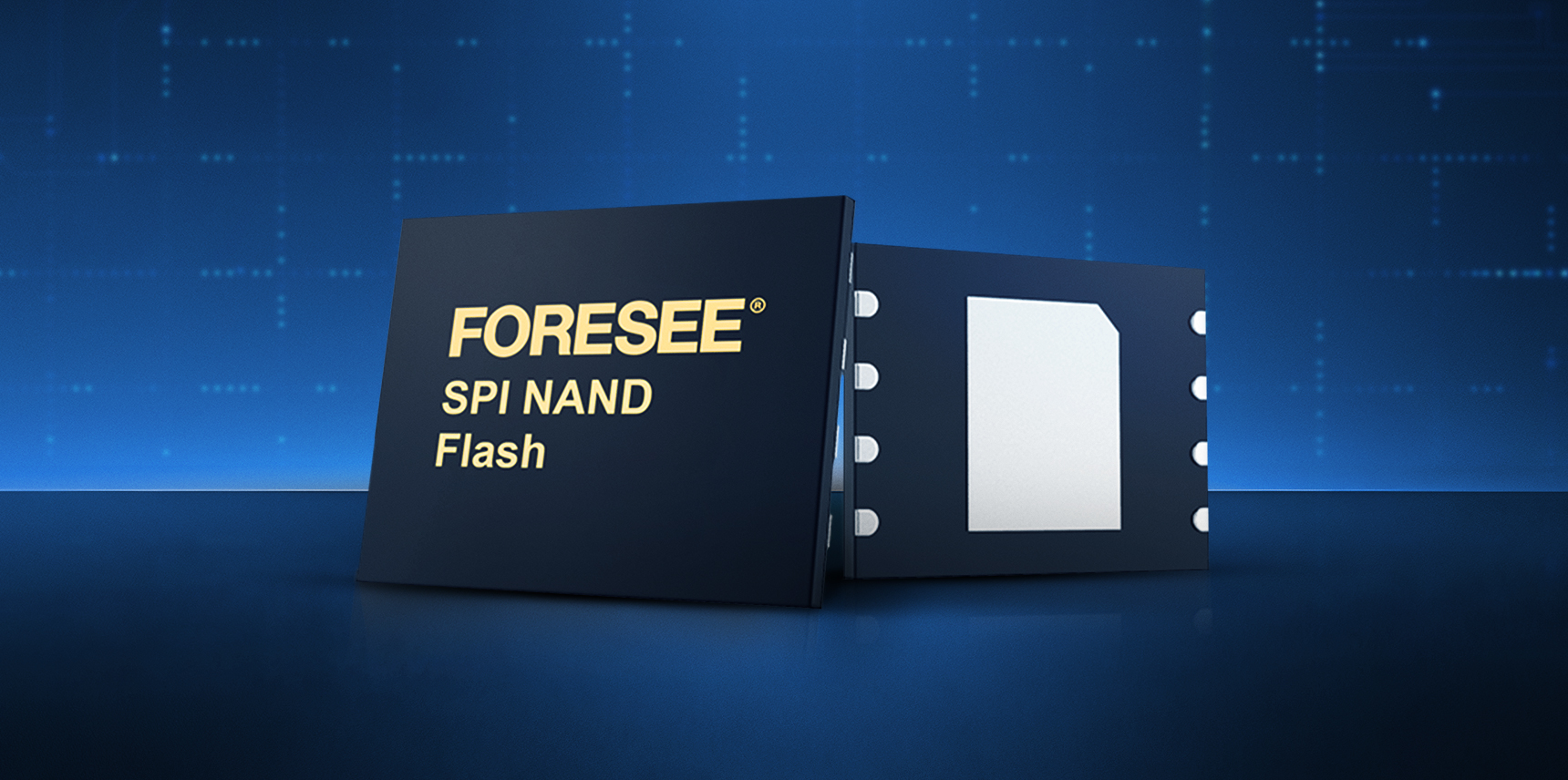
- SPI NAND Flash: A simple, low-pin-count interface (4 or 8 signal lines) suitable for smaller embedded systems where cost and PCB complexity matter more than raw throughput. SPI NAND operates at tens of megabytes per second, adequate for firmware storage, configuration data, and low-bandwidth logging. The simplicity of SPI makes it accessible for microcontroller-based designs without dedicated memory controllers.
- eMMC (embedded MultiMediaCard): A managed NAND solution with an integrated controller on the same package. eMMC presents a standard MMC interface to the host, abstracting all NAND management operations. eMMC 5.1 delivers sequential read speeds up to approximately 250MB/s and write speeds up to 125MB/s. The managed nature of eMMC – with built-in wear leveling, ECC, and bad block management – simplifies integration for automotive infotainment, instrument clusters, and industrial HMI systems.
- UFS (Universal Flash Storage): The highest-performance embedded storage interface, designed to replace eMMC in performance-demanding applications. UFS uses a serial MIPI M-PHY interface with full-duplex operation, enabling simultaneous reads and writes. UFS 3.1 achieves sequential read speeds exceeding 2,000MB/s, making it appropriate for ADAS systems processing high-resolution sensor data, high-frame-rate dashcam recording, and next-generation automotive infotainment platforms.
For a detailed comparison of interface tradeoffs in automotive embedded storage, see our guide on understanding eMMC storage and the technical breakdown in our eMMC vs SSD comparison.
Embedded NAND Flash for IIoT and Edge Applications
Industrial Internet of Things (IIoT) edge devices impose a distinct set of NAND flash requirements compared to automotive applications. Where automotive NAND prioritizes AEC-Q100 qualification and long lifecycle availability, IIoT edge storage often emphasizes low-power operation, small form factors, and resistance to write-heavy data logging workloads.
Common IIoT edge applications that rely on NAND flash memory include:
- Factory automation controllers: PLCs and industrial computers logging equipment state, event data, and production metrics continuously across multi-year deployments.
- Smart grid and utility monitoring: Remote terminal units (RTUs) and intelligent electronic devices (IEDs) that operate unattended in outdoor environments across wide temperature ranges.
- Medical device storage: Diagnostic equipment, patient monitoring systems, and portable medical devices requiring NAND flash that meets both technical endurance requirements and regulatory traceability standards.
- Surveillance and security systems: IP cameras and NVRs with continuous write workloads that can consume SSD endurance rapidly if TLC or QLC NAND is incorrectly specified.
- Edge AI inference hardware: Edge computing nodes running on-device inference models that require fast, low-latency storage for model weights and intermediate data.
For power-sensitive IIoT applications, NAND flash interfaces matter beyond just bandwidth. eMMC’s single-lane interface draws less power than multi-lane UFS configurations – a relevant consideration for battery-powered or energy-harvesting edge devices. SPI NAND remains viable for the lowest-power microcontroller-based designs where kilobytes, not gigabytes, define the storage requirement.
Battery-powered field devices, remote environmental sensors, and asset trackers go a step further – they add form factor constraints, multi-year battery life targets, and deployment environments where maintenance access is limited or impossible. These requirements shape NAND flash selection in ways that go beyond standard IIoT SSD specs. For a full breakdown of how power budgets, endurance calculations, ruggedization requirements, and interface tradeoffs apply specifically to connected device deployments, see our guide on embedded NAND flash for IoT devices.
Selecting NAND Flash Memory: A Specification Checklist for Engineers
When NAND flash memory enters a design review, these parameters should be confirmed before a component is locked into the BOM:
- Cell type vs. write workload: Calculate estimated DWPD based on application write patterns. Confirm the NAND type’s P/E cycle rating is appropriate for the design lifetime.
- Temperature qualification: Verify the component is rated for your operating temperature range. Confirm whether the temperature rating reflects junction temperature or ambient, and at what derating.
- AEC-Q100 grade: For automotive applications, confirm which AEC-Q100 grade the component is qualified to, and request the supporting qualification data package.
- Interface compatibility: Match the interface (SPI NAND, eMMC, UFS) to the host SoC’s supported memory interfaces and available bus throughput.
- ECC strength: Confirm the controller’s ECC capability meets the bit error rate requirements of your endurance target at end-of-life conditions.
- Power Loss Protection: For write-intensive applications, confirm whether PLP capacitors are included or if firmware-based PLP is implemented.
- Lifecycle availability: Request a product lifecycle timeline from the supplier. Automotive and defense programs require confirmed availability for 10-15 years minimum.
- Form factor: Confirm package dimensions, ball pitch (for BGA), and footprint compatibility with your PCB layout constraints.
For a technical comparison of SSD vs embedded NAND form factors for different industrial applications, the eMMC vs SSD guide covers the key differentiation criteria for design engineers.
NOR vs NAND Flash Memory: Choosing the Right Architecture
Engineers encountering both NOR and NAND flash in component catalogs sometimes face questions about which architecture fits a given application. The distinction matters most at the firmware and code storage layer.
NOR flash supports byte-level random access and in-place code execution (XIP), making it the standard choice for bootloader storage and small embedded firmware images where the processor reads directly from flash without loading to RAM. NOR flash endurance (10,000 to 100,000 P/E cycles depending on the device) is generally adequate for firmware update scenarios where write frequency is low.
NAND flash is optimized for large sequential data storage and cannot execute code directly without a memory controller and software abstraction layer. For storage capacities above a few megabytes – operating system images, application data, log files, media storage – NAND flash delivers better cost, density, and write throughput than NOR.
Many embedded systems use both: NOR for the primary bootloader and small critical firmware, NAND (via eMMC or UFS) for the operating system, application software, and data storage. This architecture combines the XIP advantages of NOR with the density and cost advantages of NAND.
Frequently Asked Questions About NAND Flash Memory
What is NAND flash memory used for in industrial applications?
NAND flash memory is used as the primary storage medium in industrial SSDs, eMMC modules, UFS components, and SPI NAND devices. Industrial applications include automotive ECUs, ADAS systems, IIoT edge nodes, factory automation controllers, medical devices, surveillance systems, and defense electronics. Its non-volatile data retention, high density, and improving cost-per-bit make it the dominant storage technology across these sectors.
How does NAND flash memory work at the cell level?
NAND flash stores data by trapping electrons in the floating gate or charge-trap layer of a transistor. The presence or absence of charge – and in MLC/TLC/QLC, the precise charge level – represents stored bits. Reading data applies a voltage to the control gate and senses whether current flows based on the cell’s charge state. Writing (programming) injects electrons into the floating gate using Fowler-Nordheim tunneling. Erasing removes electrons via the same mechanism, resetting the block to a known state before rewriting.
What is the difference between SLC and TLC NAND flash memory?
SLC NAND stores one bit per cell using two voltage states, delivering endurance ratings of 50,000 to 100,000 P/E cycles and the fastest read/write speeds. TLC NAND stores three bits per cell using eight voltage states, reducing cost-per-bit substantially but limiting endurance to 300 to 1,000 P/E cycles. For automotive and write-intensive industrial applications, SLC or pSLC is specified. For read-heavy applications like infotainment content storage or HMI interfaces, TLC provides adequate endurance at lower cost.
What does AEC-Q100 mean for NAND flash memory?
AEC-Q100 is the Automotive Electronics Council’s qualification standard for integrated circuits used in automotive applications. It defines stress tests including High Temperature Operating Life (HTOL), temperature cycling, humidity testing, and Early Life Failure Rate (ELFR). NAND flash memory and embedded storage components used in automotive ECUs, ADAS systems, and infotainment units should meet AEC-Q100 Grade 1 (-40°C to +125°C) or the appropriate grade for the mounting location and thermal environment.
How do I calculate NAND flash endurance for my application?
Start with your application’s daily write volume in gigabytes. Multiply by the design lifetime in days. Divide by the NAND component’s rated capacity. Factor in Write Amplification Factor (WAF) – typically 1.5 to 3x for SSDs, lower for managed eMMC/UFS with optimized firmware. Compare the result against the NAND type’s P/E cycle rating. If the calculated P/E cycles exceed the rating, move to a higher-endurance cell type or increase over-provisioning to reduce WAF.
What is 3D NAND flash memory?
3D NAND flash stacks memory cell layers vertically rather than shrinking cell dimensions to increase density. By building upward (64, 96, 128, 176+ layers depending on generation), manufacturers achieve higher storage capacity per die while using larger, more reliable cell geometries than late-generation planar NAND. Industrial-grade 3D NAND is qualified for extended temperature ranges and offers improved data retention compared to 2D NAND at equivalent density points.
What is the difference between eMMC and UFS embedded NAND storage?
Both eMMC and UFS are managed embedded NAND storage standards with integrated controllers. eMMC uses a parallel bus interface with half-duplex operation, achieving sequential read speeds up to approximately 250MB/s in the eMMC 5.1 specification. UFS uses a serial MIPI interface with full-duplex operation, reaching over 2,000MB/s sequential reads in UFS 3.1 – making UFS the appropriate choice for ADAS sensor data processing, high-resolution dashcam recording, and next-generation automotive infotainment. For detailed interface comparison, see our eMMC storage guide.
Why is NAND used in storage devices instead of other memory types?
NAND flash offers the best combination of storage density, non-volatile data retention, and cost-per-bit among available solid-state storage technologies. Compared to DRAM, NAND retains data without power. Compared to NOR flash, NAND delivers higher density and write throughput. Compared to emerging technologies like MRAM or ReRAM, NAND flash has decades of manufacturing maturity, established supply chains, and proven reliability data across industrial and automotive environments.
NAND Flash Memory Solutions from Lexar Enterprise
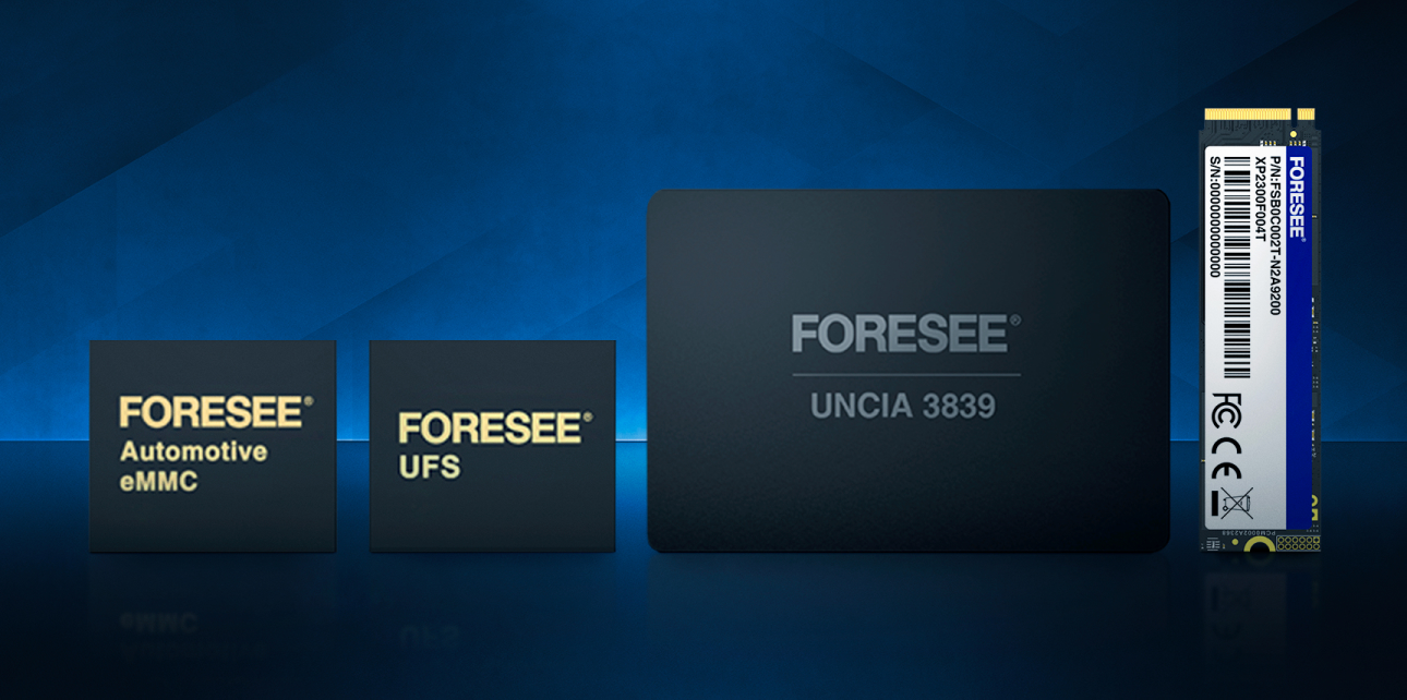
Lexar Enterprise, operating under the FORESEE brand for embedded and industrial storage, offers NAND flash memory solutions spanning SPI NAND, eMMC 5.1, UFS 3.1, and industrial SSD form factors. Products are qualified for extended temperature operation and backed by the component lifecycle availability commitments that automotive OEM and industrial computing programs require.
Engineering teams can access datasheets, qualification summaries, and application-specific configuration guides through the Lexar Enterprise technical resource library. For sample requests or design-in support, contact our industrial memory team directly.
- Explore embedded storage products including SPI NAND, eMMC, and UFS modules
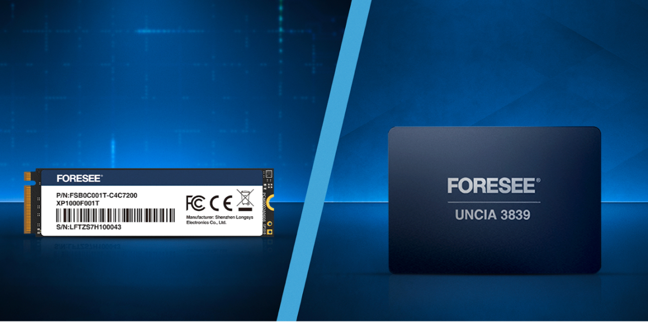
- View industrial SSD solutions for high-capacity, high-endurance applications
- Review automotive NAND flash specifications for AEC-Q100 qualified components
If you’re specifying NAND flash memory for an upcoming design and need to confirm component qualification data, endurance ratings, or interface compatibility – contact the Lexar Enterprise engineering support team to begin the evaluation process.