
Advanced Driver Assistance Systems (ADAS) have moved from optional safety add-ons to the core architecture of modern vehicles. If you’re designing memory into an ADAS subsystem – whether that’s a camera ECU, a domain controller, or a full-stack L4 compute platform – the memory requirements are non-trivial. ADAS memory requirements span low-latency DRAM for real-time processing, high-endurance NAND flash for data logging, and embedded solutions like LPDDR5, eMMC, and UFS that must survive -40°C to +125°C without flinching.
This guide covers what engineers actually need to specify: bandwidth numbers by autonomy level, AEC-Q100 temperature grades, ASIL requirements, and the data volumes that ADAS sensor stacks generate. The goal is to give you the technical reference that most automotive memory explainers skip.
What Is ADAS (Advanced Driver Assistance Systems)?
ADAS – short for Advanced Driver Assistance Systems – refers to the collection of sensing, processing, and actuation technologies that help vehicles monitor their environment and work alongside or override driver inputs to improve safety. The acronym ADAS full form covers a broad spectrum: from simple rear-view cameras and lane departure warnings in Level 1 vehicles, to the sensor fusion platforms and neural network inference engines that power Level 4 robotaxi fleets.
ADAS was first introduced in production vehicles in the early 1990s, with anti-lock braking systems (ABS) and electronic stability control (ESC) representing the earliest driver assistance functions. By the early 2000s, adaptive cruise control and forward collision warning entered production vehicles from Mercedes-Benz and Toyota. Today, ADAS technology is standard equipment across most new vehicle platforms globally, with NHTSA reporting that automatic emergency braking alone is projected to prevent tens of thousands of crashes annually as it becomes universal across fleets – according to the NHTSA Automated Vehicles Safety program.
Key ADAS Functions and Their Data Volume
Each ADAS function generates and consumes data at different rates. Understanding the data volume by function is the first step in specifying the right memory architecture:
- Collision Avoidance and Automatic Emergency Braking (AEB) – Processes radar and camera feeds to detect obstacles, requiring sub-10ms reaction latency. Memory must support continuous streaming reads from radar processors.
- Lane Departure Warning and Lane Keep Assist – Continuously analyzes forward camera feeds at 30-60fps, generating 1.5-3 Gbps of raw image data per camera stream per second.
- Adaptive Cruise Control (ACC) – Relies on forward radar and camera fusion with low-latency DRAM access for real-time speed regulation.
- Traffic Sign Recognition – Runs convolutional neural network inference on camera frames, requiring high memory bandwidth for weight loading and activation storage.
- Parking Assistance and Surround-View – Fuses data from 4-8 cameras plus ultrasonic sensors simultaneously, requiring parallel memory access from multiple streams.
- LiDAR Point Cloud Processing – Generates 10-100 million data points per second depending on sensor resolution, requiring high-bandwidth DRAM and fast NVMe storage for logging.
ADAS Levels: From L1 Driver Assistance to L5 Full Autonomy
The SAE J3016 standard defines six levels of driving automation (L0 through L5). Each level carries distinct memory requirements because higher autonomy levels require more sensors, more compute, and faster data pipelines:
| SAE Level | Description | Primary Memory Type | Typical Bandwidth Requirement |
|---|---|---|---|
| L0 | No automation (alerts only) | Basic SRAM/Flash | Low (<1 GB/s) |
| L1 | Single function assistance (AEB, ACC) | LPDDR4, eMMC | 5-20 GB/s |
| L2 | Combined function (lane + speed control) | LPDDR4X, UFS 3.1 | 20-50 GB/s |
| L3 | Conditional automation (driver on standby) | LPDDR5, GDDR6, NVMe | 100-256 GB/s |
| L4 | High automation (geo-fenced self-driving) | GDDR6 at 16 Gbps, HBM2 | 256-512 GB/s |
| L5 | Full automation (any environment) | HBM2E, GDDR6X, NVMe RAID | 512 GB/s – 1024 GB/s |
The 512 GB/s to 1024 GB/s bandwidth figure for L3/L4 platforms is consistent with published technical analysis from semiconductor companies designing for autonomous driving workloads. For context, GDDR6 at 16 Gbps provides roughly 64 GB/s per device – meaning L4 systems may require 8-16 GDDR6 devices to meet bandwidth targets, or alternative high-bandwidth memory architectures.
How ADAS Collects and Processes Data
ADAS data collection is a pipeline problem. Raw sensor data arrives asynchronously from multiple sources, must be timestamped and synchronized, processed through perception algorithms, and acted upon – all within the latency budget of the safety function being executed. For AEB, that budget is under 100ms from object detection to brake application. For lane-keeping, it’s similar. This pipeline requires memory at every stage.
Sensor Stack: Cameras, Radar, LiDAR, and Ultrasonic
A representative ADAS sensor stack for an L2+ production vehicle typically includes:
- 6 HD cameras (forward, rear, and side views) – each producing approximately 1.5 Gbps of raw image data
- 4 ultrasonic sensors – low data rate, primarily for near-field parking and proximity alerts
- 2 forward-facing radar units – medium data rate, continuous distance and velocity measurement
- 1 LiDAR unit (present in L3+ vehicles) – high data rate, 10-100M points/second depending on resolution
A 6-camera + 4-ultrasonic + 2-radar configuration generates approximately 40+ GB of raw sensor data per hour of driving. This figure scales rapidly with sensor count and resolution upgrades. L4 platforms with high-resolution LiDAR and additional camera channels can generate hundreds of GB per hour, which creates real pressure on both on-vehicle NAND storage and the automotive memory bandwidth available at the ECU level.
Data Volume Reality: How Much Data ADAS Generates
The data volume produced by ADAS sensor stacks is one of the most common points of underestimation in early-stage system design. Engineers working on ADAS storage requirements need to plan for:
- Real-time processing buffer – DRAM sized for the maximum concurrent sensor data that must be held in memory during processing windows
- Event-triggered logging – NAND flash capacity for edge-case and incident recording (the “black box” function)
- Map and HD map storage – L3+ systems relying on HD map localization require tens of GB of map data onboard
- OTA update partitions – Software-defined vehicles require reserved storage for over-the-air firmware and model updates, often in the gigabyte to multi-gigabyte range per ECU
- Training data offload – Some OEMs collect sensor data for ML training; vehicles with this function may log TBs of data over their service life
For engineers specifying ADAS data storage at the system level, plan for a minimum of 64-256 GB of onboard NAND flash for L2+ platforms, scaling to terabyte-class NVMe storage for L4 compute platforms.
Types of Automotive Memory for ADAS
ADAS systems use multiple memory types simultaneously, each serving a specific function in the data pipeline. Understanding the role of each type is essential for specifying the right solution.
DRAM: Low-Latency Processing for Real-Time Decisions
DRAM is the working memory of an ADAS system – it holds the data actively being processed by the ADAS SoC or domain controller. For automotive applications, DRAM must be automotive-grade, meaning it is qualified for the temperature ranges and vibration environments found in vehicle installations.
LPDDR4X is the current production standard for L1-L2 ADAS ECUs. Lexar Enterprise also offers automotive-grade LPDDR4 memory for designs where LPDDR4X meets the bandwidth requirement at lower system cost. LPDDR5 – which offers approximately 1.5x the bandwidth of LPDDR4X – is entering production in L2+ and L3 systems. For L3-L4 compute platforms that run neural network inference, GDDR6 at 16 Gbps per pin provides substantially higher bandwidth for the matrix operations that deep learning workloads require.
Key DRAM specifications for ADAS applications:
- Operating temperature – Automotive DRAM must be AEC-Q100 Grade 1 qualified (-40°C to +125°C junction temperature)
- Data retention – DRAM loses state when unpowered; stored state must be offloaded to NAND flash or NOR flash
- ECC support – Error-correcting code memory is required for safety-critical ADAS functions to detect and correct single-bit errors
- Bandwidth per device – LPDDR5 reaches up to ~44 GB/s per channel; GDDR6 reaches ~64 GB/s per device at 16 Gbps
Lexar Enterprise LPDDR5 memory is designed for embedded automotive and industrial applications that require low power consumption alongside high-bandwidth performance.
NAND Flash: Long-Term Storage and Data Logging
NAND flash provides the non-volatile storage layer in ADAS – it retains data when power is removed, making it essential for firmware storage, HD maps, event logging, and OTA update staging. For ADAS sensor data storage, NAND flash endurance and temperature ratings are the primary specification concerns.
SLC (Single-Level Cell) NAND offers the highest endurance – typically 100K+ program/erase cycles – and the widest operating temperature range, making it the preferred choice for safety-critical ADAS data logging applications. MLC and TLC NAND provide higher density at lower cost but with reduced endurance (3K-10K P/E cycles for TLC), which may be acceptable for less write-intensive applications like map storage. For a full comparison of endurance and temperature behavior across SLC, MLC, TLC, and QLC, see the analysis of NAND flash cell types for automotive and industrial applications.
For automotive applications, NAND flash memory for automotive must meet the endurance, temperature, and reliability requirements of AEC-Q100 qualification. Lexar Enterprise SLC SPI NAND Flash provides the P/E cycle counts and temperature ratings required for ADAS event logging and firmware storage applications.
Embedded Memory: LPDDR, eMMC, UFS, and SSD Solutions
Embedded memory solutions package flash storage and a controller into a single managed device, simplifying integration in ADAS ECUs:
- eMMC (embedded MultiMediaCard) – Industry-standard for L1-L2 ADAS ECUs and TCUs. eMMC 5.1 supports sequential read speeds up to 250-300 MB/s. Automotive-grade eMMC must meet AEC-Q100 qualification. Lexar Enterprise automotive eMMC solutions are validated for automotive temperature ranges and endurance requirements.
- UFS (Universal Flash Storage) – Higher performance than eMMC, with UFS 3.1 supporting sequential reads up to 2100 MB/s and command queue support for concurrent read/write operations. For a detailed side-by-side breakdown of interface speeds and write latency, see the UFS vs eMMC performance comparison. For automotive-specific deployment considerations, Lexar Enterprise covers both in their UFS and eMMC automotive solutions guide. Used in higher-end ADAS domain controllers.
- NVMe SSD – M.2 or custom form factor NVMe SSDs are used in L3-L4 compute platforms for high-speed data logging and map storage. Automotive SSD storage solutions for ADAS must be vibration-rated and temperature-qualified to automotive standards.
NOR Flash: Boot Code and Safety-Critical Firmware
NOR flash occupies a specific and non-negotiable role in ADAS: it stores the boot code and safety-critical firmware that the ADAS SoC executes at startup. Unlike NAND flash, NOR flash supports random read access at the byte level, which is required for XIP (execute-in-place) operations where code runs directly from flash without first being loaded into DRAM.
NOR flash specifications relevant to ADAS applications include random read speeds up to 104 MB/s, latency as low as 50 ns, and support for Octal SPI, Quad SPI, and Parallel NOR interfaces. Lexar Enterprise offers SPI and xSPI NOR Flash for automotive boot storage with the interface options and temperature ratings required for ADAS boot code applications. Endurance for NOR flash used in ADAS firmware storage is typically 100K+ program/erase cycles with 20-year data retention at operating temperature.
AEC-Q100 and Automotive Memory Standards
AEC-Q100 is the Automotive Electronics Council’s stress test qualification standard for integrated circuits intended for use in automotive applications. For memory components in ADAS systems, AEC-Q100 qualification is not optional – it is the baseline requirement for any component that will operate in a vehicle environment. AEC-Q100 is part of a broader automotive memory validation testing process that includes system-level integration and thermal cycling verification. An overview of AEC-Q100 specifications and test requirements is available from suppliers who publish technical documentation on the AEC-Q100 standard.
AEC-Q100 Temperature Grades for ADAS Applications
AEC-Q100 defines five temperature grades. For ADAS applications, Grade 1 and Grade 2 are the most commonly specified:
| AEC-Q100 Grade | Ambient Temperature Range | Typical ADAS Application |
|---|---|---|
| Grade 0 | -40°C to +150°C | Engine bay, transmission control (rarely memory) |
| Grade 1 | -40°C to +125°C | Under-hood ADAS ECUs, domain controllers near heat sources |
| Grade 2 | -40°C to +105°C | Passenger compartment ADAS ECUs, infotainment-adjacent systems |
| Grade 3 | -40°C to +85°C | Interior-only applications (not suitable for ADAS) |
For ADAS memory components, AEC-Q100 Grade 1 is the standard specification for any ECU that may be located in or near the engine compartment, door modules, or areas exposed to direct sun loading. Grade 2 (-40°C to +105°C) may be acceptable for passenger compartment-mounted control units where ambient temperatures are managed by the vehicle HVAC system, but engineers should verify the specific thermal environment before downgrading from Grade 1.
The -40°C lower bound is equally important. Cold-start performance of ADAS systems is a functional safety requirement – a vehicle starting in a winter environment at -40°C must have ADAS functions available within the system initialization window.
ISO 26262 Functional Safety and ASIL Levels
ISO 26262 is the international functional safety standard for road vehicles. It defines the processes and requirements for developing safety-related electrical and electronic systems in vehicles. For ADAS memory components, ISO 26262 compliance means the memory solution must be characterized for its failure modes and the system must be designed to tolerate or detect those failures.
ISO 26262 defines four Automotive Safety Integrity Levels (ASIL A through ASIL D), with ASIL D representing the most stringent safety requirements. ADAS functional safety and ASIL requirements vary by function:
- ASIL D – Automatic Emergency Braking (AEB) actuation, electronic power steering with ADAS override. Memory used in these paths must support error detection and correction (ECC).
- ASIL C – Lane Keep Assist actuation, adaptive cruise control with brake authority. ECC memory and redundant storage paths are required.
- ASIL B – Forward collision warning, lane departure warning (alert-only). Lower memory integrity requirements but still requires documented failure mode analysis.
- ASIL A – Driver monitoring systems, comfort-level ADAS functions. Baseline safety requirements apply.
ADAS compliance with ISO 26262 requires that memory suppliers provide FMEA (Failure Mode and Effects Analysis) documentation and safety manuals for their components. Engineers specifying AEC-Q100 memory for safety-critical ADAS paths should confirm that the supplier provides ISO 26262 Part 11 (semiconductor guidelines) documentation.
Endurance, Data Retention, and ESD Protection Requirements
Beyond temperature grades and functional safety certification, automotive memory for ADAS must meet specific endurance and retention targets:
- Program/Erase (P/E) cycles – SLC NAND for ADAS data logging should provide 100K+ P/E cycles minimum. For TCU firmware storage, 100K P/E cycles with wear leveling is the standard.
- Data retention – Automotive NAND and NOR flash must retain data for a minimum of 10 years at operating temperature. Some OEM specifications require 20-year retention for safety firmware storage.
- ESD protection – Automotive memory must meet HBM (Human Body Model) and CDM (Charged Device Model) ESD protection requirements per AEC-Q100 test conditions.
- EMC compliance – ADAS ECU memory must meet ISO 11452 electromagnetic compatibility requirements to avoid interference with vehicle communication buses and safety systems.
Technical Specifications: What Engineers Should Specify
When writing a memory specification for an ADAS subsystem, vague requirements like “high speed” or “reliable” create supply chain risk and integration problems. Here are the technical parameters engineers should specify by application.
Bandwidth Requirements by ADAS Function
Automotive memory bandwidth requirements vary significantly across ADAS functions and autonomy levels. The following figures are derived from published semiconductor industry data and ADAS platform architectures:
- Camera ISP processing – Each HD camera stream at 1.5 Gbps requires roughly 190 MB/s of sustained memory bandwidth for ISP processing. A 6-camera system requires approximately 1.1 GB/s minimum from LPDDR memory.
- Radar signal processing – Forward radar at 77 GHz with 4D imaging generates 10-100 MB/s of data depending on range resolution and update rate. Low bandwidth relative to cameras, but requires very low latency.
- LiDAR point cloud processing – High-resolution LiDAR (128-channel) generates 100-200 MB/s of point cloud data. Processing this data through 3D object detection algorithms is memory-bandwidth-intensive.
- Neural network inference – Object detection models (YOLO variants, ResNet derivatives) require loading weight matrices from memory for each inference pass. Batch sizes, model size, and inference frequency determine the effective bandwidth requirement. For L2+ camera perception running at 30fps, this is typically 5-20 GB/s sustained.
- Sensor fusion – Combining radar, camera, and LiDAR data in a shared object model requires random-access memory operations across large buffers. Peak memory bandwidth for a full sensor fusion pipeline in an L3 domain controller is in the 100+ GB/s range.
Temperature Operating Range (-40°C to +125°C)
All memory components in ADAS applications should be specified to the full AEC-Q100 Grade 1 range of -40°C to +125°C unless the thermal environment has been measured and documented to support a narrower grade. Specific thermal design considerations:
- Junction temperature vs. ambient – The AEC-Q100 grade refers to junction temperature. For high-power ADAS SoCs with co-packaged memory, the memory junction temperature may be significantly higher than ambient. Thermal simulation or testing is required to validate the actual operating temperature.
- Cold-start initialization – At -40°C, NAND flash write latency increases significantly (typically 2-5x vs. room temperature). ADAS systems must account for extended cold-start initialization times in their boot sequence design.
- Thermal derating – NAND flash endurance degrades at high temperatures. Operating continuously at +125°C junction temperature accelerates wear relative to room-temperature endurance specifications. Review the supplier’s temperature-endurance derating curves when designing for worst-case thermal environments.
Power Consumption and Thermal Design Considerations
Power consumption is a material design constraint for ADAS, particularly in battery electric vehicles where every watt of continuous consumption has a direct impact on range. Representative power figures for ADAS compute and memory components:
- High-performance ADAS SoC (e.g., NVIDIA DRIVE Orin class) – 45-65W peak SoC power, with GDDR6 memory adding 5-10W per device
- Domain controller CPU – Automotive-grade high-performance CPUs draw 100-350W depending on core count and configuration
- NVMe SSD storage – Automotive NVMe SSDs in active write mode draw 15-20W; idle power is typically 3-5W
- eMMC/UFS embedded storage – Active power 200-500mW; idle <50mW – significantly more power-efficient than NVMe for lower-throughput applications
- LPDDR5 – Roughly 30-40% lower power than LPDDR4X at equivalent bandwidth, a key advantage for battery electric ADAS platforms
For EV platforms, specifying LPDDR5 over LPDDR4X in ADAS ECUs provides meaningful system-level power savings when multiplied across dozens of ECUs operating continuously over the vehicle lifetime. For firmware-level techniques to reduce storage power draw, see the guide on SSD power optimization strategies for embedded systems.
ADAS Processors, SoCs, and Memory Architecture
ADAS data processing architecture is dominated by a set of purpose-built automotive SoCs designed for sensor fusion, neural network inference, and real-time safety processing. The ADAS processor and memory subsystem are tightly coupled – memory selection must match the SoC’s memory interface capabilities:
- NVIDIA DRIVE Orin – 254 TOPS AI performance, supports LPDDR5 memory at up to 204.8 GB/s aggregate bandwidth. The production SoC for L2+ through L4 ADAS platforms from multiple OEMs.
- Qualcomm Snapdragon Ride – Multi-chip scalable platform targeting L2+ through L4, supporting LPDDR5 memory interfaces and NVMe storage for data logging.
- Mobileye EyeQ6 – Purpose-built for computer vision ADAS functions, LPDDR5 memory interface, optimized for camera-centric perception stacks.
- Texas Instruments TDA4 – Designed for L2-L3 ADAS applications including surround-view camera processing and sensor fusion, supports LPDDR4X and LPDDR5 memory.
When specifying ADAS memory, confirm that the chosen DRAM type and speed grade matches the memory controller specification of the target SoC. LPDDR5 channels must be routed according to the SoC’s PCB layout guidelines to achieve rated bandwidth.
AI, Machine Learning, and Edge Computing in ADAS
The shift toward AI-driven ADAS has changed the memory requirements conversation. First-generation ADAS relied on deterministic algorithms with predictable memory access patterns. Modern neural network-based perception systems have irregular memory access patterns driven by model architecture – loading large weight tensors, storing intermediate activation maps, and performing high-bandwidth matrix multiplications across millions or billions of parameters.
Neural Network Memory Requirements
Deep neural network models used for ADAS object detection and segmentation range from a few MB (MobileNet-class models for constrained ECUs) to several GB (larges for L4 perception stacks). The memory implications:
- Model weight storage – Weights are stored in NAND flash and loaded into DRAM at runtime. A 300MB detection model occupying DRAM continuously represents a material portion of total DRAM on a constrained ECU.
- Activation memory – Intermediate layer activations during inference require scratch memory proportional to model size and batch size. This is pure DRAM consumption during inference.
- Inference latency vs. bandwidth – For real-time ADAS, reducing inference latency is often more important than throughput. High-bandwidth DRAM reduces the time spent loading weights and activations, directly reducing per-frame inference latency.
ADAS Data Processing: Edge vs. Cloud Storage Architecture
How data is handled in advanced driver assistance systems is determined by the latency requirements of each function. Safety-critical functions – AEB, lane keep assist, collision warning – cannot tolerate the round-trip latency of cloud-based processing. They must run entirely on-vehicle, within the latency budget of the specific function.
Cloud computing in ADAS serves a different role: it receives logged driving data from the vehicle over cellular connectivity, processes it for fleet-level analytics, and delivers software and model updates back to the vehicle via OTA. The memory implication is that ADAS storage must accommodate OTA staging partitions large enough to hold full firmware images – often in the gigabyte range per ECU, and potentially multi-gigabyte for compute platforms running large AI models.
Software-Defined Vehicles and OTA Update Storage
The Software-Defined Vehicle (SDV) architecture is the most significant structural change in automotive system design in the current decade. In an SDV, vehicle functions – including ADAS behavior – are defined and updated through software rather than requiring hardware changes. This has direct implications for ADAS memory specifications:
- Dual-bank OTA partitions – SDV ECUs require at least two full firmware partitions so that an OTA update can be staged in the inactive partition while the active partition continues running. This doubles the minimum NAND flash requirement for the firmware storage area.
- Model update packages – When ADAS perception models are updated via OTA, the update package must fit in staging storage. Large model updates can be several GB in size.
- Rollback storage – Safe OTA requires the ability to roll back to a known-good firmware version. Additional NAND capacity must be reserved for rollback images.
- Secure boot integration – OTA updates require cryptographic verification at boot. NOR flash storing the root of trust (secure boot keys and initial boot code) must be write-protected after initial provisioning.
Challenges in ADAS Memory Performance
Data Throughput at Scale
As sensor counts and resolutions increase with each ADAS generation, the data throughput challenge grows proportionally. A high-resolution 8MP camera operating at 30fps generates roughly 2-3x the data of a 2MP camera at the same frame rate. Multi-camera L3 platforms are now managing aggregate sensor data rates that challenge the sustained write throughput of embedded storage solutions. Engineers must specify storage with write throughput headroom above the sustained sensor data rate – sustained write speeds of 500+ MB/s are required for high-resolution multi-camera logging applications.
Power Efficiency for EVs
Battery electric vehicles have intensified the focus on per-ECU power consumption. An ADAS domain controller running 20-30 ECUs continuously must manage aggregate system power. Memory technology selection – LPDDR5 over LPDDR4X, UFS over NVMe for lower-throughput applications – is one of the levers available to system architects managing EV power budgets without compromising ADAS performance.
Environmental Durability and Vibration Tolerance
ADAS ECUs are mounted throughout the vehicle – in the engine bay, doors, roof, and trunk. Memory components must survive MIL-STD-810 or equivalent vibration and shock profiles, thermal cycling from -40°C to +125°C (Grade 1), humidity exposure, and the electromagnetic environment of a modern vehicle with high-voltage EV powertrain. Memory reliability is also tested during ADAS calibration procedures, where sensor calibration data must be written and read back accurately after environmental exposure. Automotive-grade memory is tested against these conditions as part of AEC-Q100 qualification – consumer or industrial-grade components without automotive qualification should not be used in ADAS applications. For a deeper look at how embedded storage survives these conditions in practice, see the guide on embedded memory for harsh environment deployments.
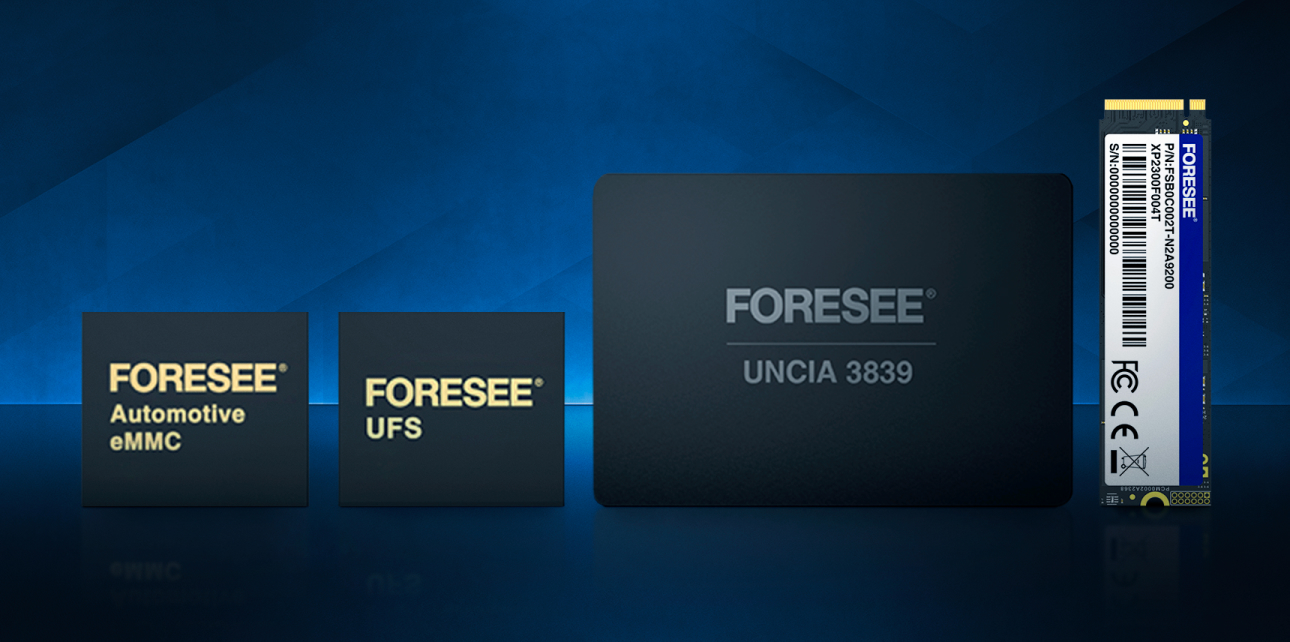
How Lexar Enterprise Memory Solutions Support ADAS
Lexar Enterprise develops and qualifies embedded memory solutions for the automotive, industrial, and embedded markets. For ADAS applications, the Lexar Enterprise product portfolio addresses the embedded storage and DRAM requirements across L1 through L3+ ADAS ECU designs:
- LPDDR5 and LPDDR5X CAMM2 – Lexar Enterprise LPDDR5 provides the bandwidth and power efficiency required for AI-driven ADAS processing, with automotive-grade temperature qualification. The LPDDR5 CAMM2 module extends this to next-generation compute platforms requiring the CAMM2 form factor.
- Automotive eMMC – Lexar Enterprise automotive-grade eMMC is validated for the temperature ranges and endurance requirements of ADAS firmware storage and data logging. For a full technical overview of eMMC in automotive applications, see the automotive eMMC application guide.
- SLC SPI and Parallel NAND Flash – Lexar Enterprise SLC NAND provides 100K+ P/E cycle endurance and automotive temperature qualification for safety-critical data logging and firmware storage. The Parallel SLC NAND Flash variant supports higher-throughput applications requiring wider bus interfaces.
- Automotive SSD Storage – Lexar Enterprise automotive SSD storage solutions cover L3+ ADAS platforms with HD map storage, event logging, and OTA staging requirements. For industrial-grade NVMe options, see the industrial SSD product range.
- NAND Flash for Automotive – Lexar Enterprise NAND flash for automotive applications covers AEC-Q100 qualification requirements and long-term availability commitments that automotive OEM design teams require for BOM planning.
Contact Lexar Enterprise for technical specifications, sample requests, and application engineering support for your ADAS memory design.
The Future of ADAS Memory Technology
The trajectory of ADAS memory requirements follows the trajectory of vehicle autonomy – more sensors, more compute, more data, more stringent memory specifications at every level of the stack.
LPDDR5 and LPDDR5X: The Next Bandwidth Generation
LPDDR5X is the next generation of low-power DRAM for embedded automotive applications, offering up to 8533 Mbps data rates – roughly double the bandwidth of LPDDR4X. For L2+ and L3 ADAS ECUs currently constrained by memory bandwidth, LPDDR5X provides the headroom needed to support higher-resolution cameras, larger AI models, and higher-frequency sensor fusion without increasing power consumption proportionally.
Next-Gen NAND Flash with Advanced ECC
As NAND process nodes shrink, raw bit error rates increase – which means the error correction code (ECC) engine in the storage controller must work harder to maintain the data integrity required by ADAS applications. Next-generation automotive NAND flash incorporates LDPC (Low-Density Parity Check) ECC, which provides significantly more error correction capability than the BCH ECC used in earlier generations. For ADAS engineers, this means higher-capacity NAND at smaller process nodes can be qualified for safety-critical applications – the ECC capability compensates for the increased error rate of smaller cells.
Memory Requirements for Fully Autonomous Fleets
L5 fully autonomous vehicles require memory architectures that don’t yet exist in production. The 512 GB/s to 1024 GB/s bandwidth requirements for L5 systems are at the edge of what current HBM2E and GDDR6X technology can deliver, and they drive system cost to levels that are not currently compatible with mass-market vehicle pricing. The memory technology development pathway for L5 includes wider HBM integration, compute-in-memory architectures that reduce the data movement bottleneck, and new interface standards that increase bandwidth-per-pin efficiency.
Fleet operators running L4 robotaxi systems today are managing terabyte-scale data flows per vehicle per day – data that must be logged, offloaded, processed for model training, and returned to the fleet as model updates. The data infrastructure requirements of an autonomous fleet extend well beyond the in-vehicle memory architecture into cloud storage, edge servers, and the cellular connectivity that links them.
Frequently Asked Questions About ADAS Memory Requirements
What is ADAS on a car?
ADAS stands for Advanced Driver Assistance Systems – the collection of sensor, compute, and actuation technologies that help vehicles detect hazards, maintain lanes, regulate speed, and automated parking and other driving functions. ADAS systems range from basic (Level 1, single function like AEB) to highly automated (Level 4, self-driving within a defined geographic area).
How does ADAS work?
ADAS works by continuously collecting data from cameras, radar, LiDAR, and ultrasonic sensors, processing that data through perception algorithms (increasingly neural network-based), and using the output to generate driver alerts or direct vehicle control inputs. The core constraint is latency – safety-critical ADAS functions must complete the full sense-process-act cycle in under 100ms, which requires high-bandwidth, low-latency memory at every stage of the pipeline.
What memory does an ADAS system need?
ADAS systems use multiple memory types: DRAM (LPDDR4X, LPDDR5, or GDDR6 depending on autonomy level) for real-time processing, NAND flash (SLC or eMMC/UFS) for firmware and data logging, NOR flash for boot code, and increasingly NVMe SSD for high-capacity logging and map storage on L3+ platforms. All memory must be AEC-Q100 qualified for automotive temperature ranges.
What is AEC-Q100 for automotive memory?
AEC-Q100 is the Automotive Electronics Council’s stress test qualification standard for integrated circuits used in automotive applications. For memory, AEC-Q100 Grade 1 qualification means the component has been tested and verified to operate reliably over the full -40°C to +125°C temperature range, through thousands of thermal cycles, vibration profiles, humidity exposure, and other automotive environmental conditions. Grade 1 is the standard specification for ADAS ECU memory components.
What is the difference between Level 2 and Level 3 ADAS memory requirements?
Level 2 ADAS (combined function, like combined lane keep and adaptive cruise) typically requires LPDDR4X DRAM at 20-50 GB/s bandwidth and eMMC or UFS storage. Level 3 ADAS (conditional automation, where the system handles all driving in defined conditions) requires significantly more memory bandwidth – 100-256 GB/s is typical – because it runs more complex sensor fusion algorithms and larger neural network models. L3 platforms often use LPDDR5 or GDDR6 DRAM, and NVMe SSD for higher-capacity logging and HD map storage.